Method for reducing defect density of gallium nitride nanowire array crystal

A technology for gallium nitride nanowires and crystal defects, which is applied in semiconductor technology and nanometer fields to solve the effect of lattice mismatch, improve crystal quality, and reduce the probability of penetration

Active Publication Date: 2014-01-22
INST OF METAL RESEARCH - CHINESE ACAD OF SCI
View PDF3 Cites 8 Cited by
  • Summary
  • Abstract
  • Description
  • Claims
  • Application Information

AI Technical Summary

Problems solved by technology

[0004] The above technologies basically use a buffer layer or a combination of buffer layers to reduce the defect density inside the GaN crystal or partially prevent the defects from propagating from the substrate to the inside of the GaN crystal, but cannot completely prevent the defects in the substrate from spreading to the crystal due to epitaxial growth. Internal propagation cannot fundamentally solve the problem of excessive defect density in GaN crystals

Method used


Image

  • Method for reducing defect density of gallium nitride nanowire array crystal
  • Method for reducing defect density of gallium nitride nanowire array crystal
  • Method for reducing defect density of gallium nitride nanowire array crystal

Examples


Embodiment 1

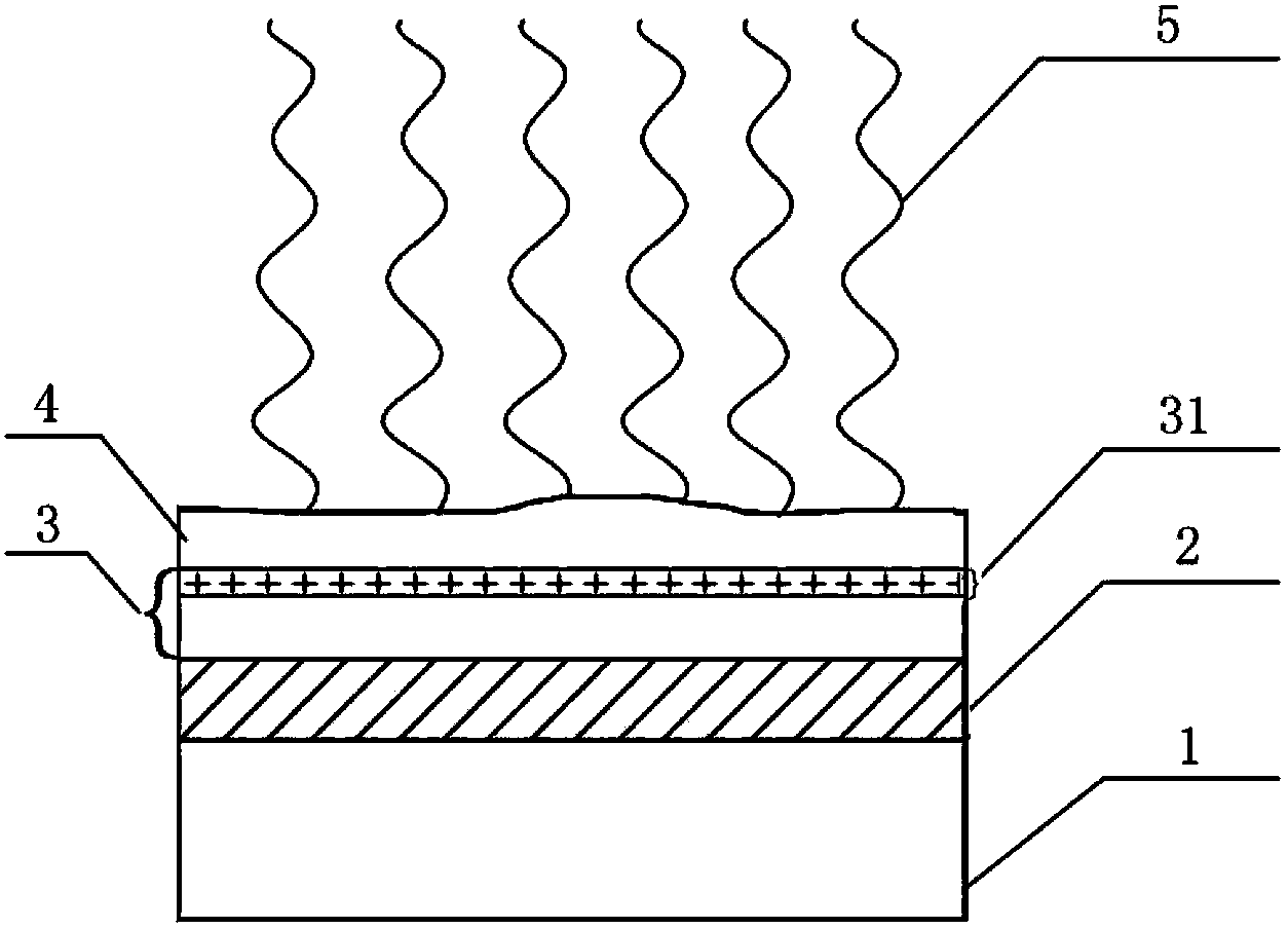
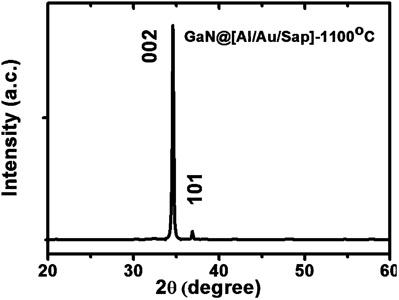
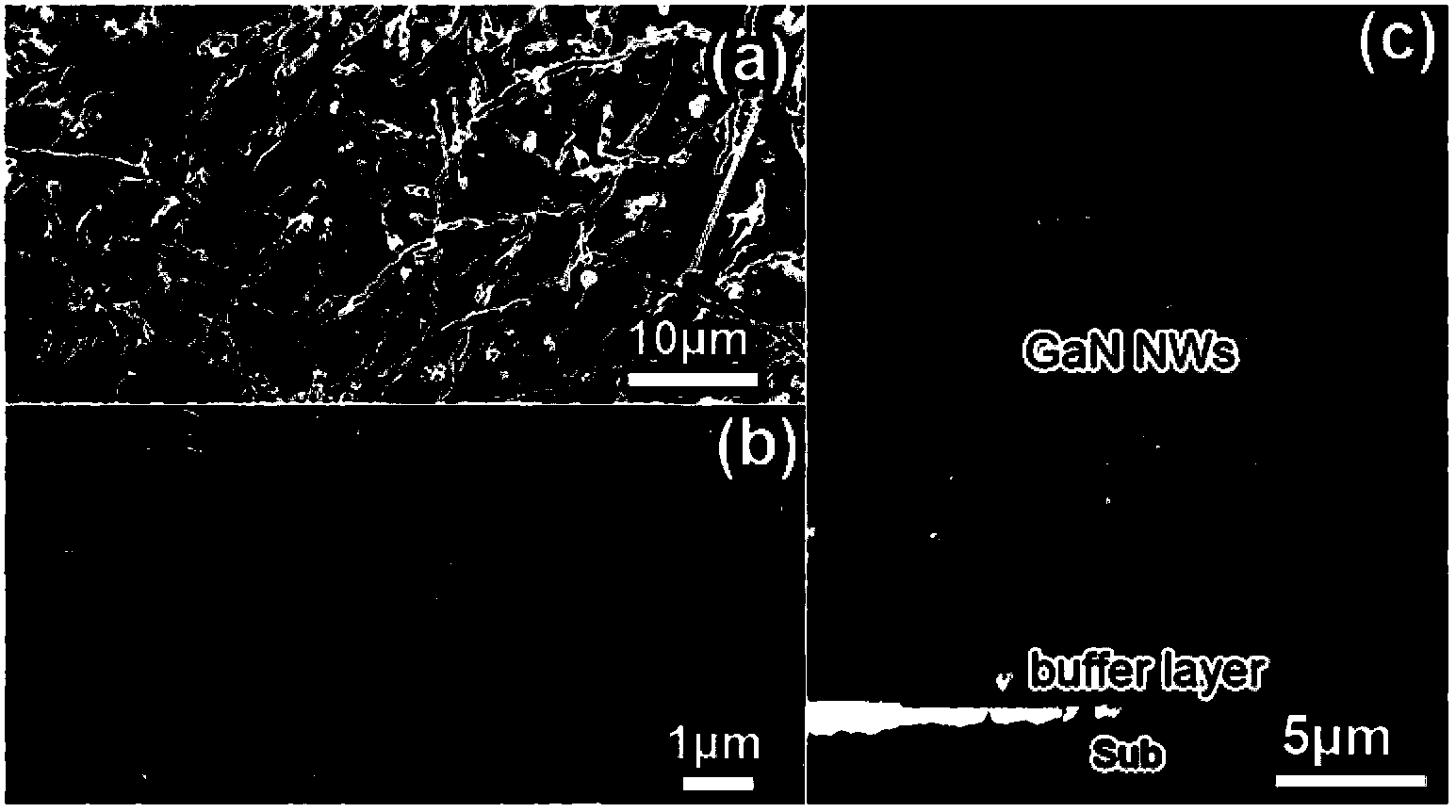
[0028] In this embodiment, an Au barrier layer and an initial Al buffer layer are deposited on a sapphire substrate to reduce the crystal defect density of a GaN nanowire array, and a GaN nanowire array is synthesized by a chemical vapor deposition method. details as follows:

[0029] 1. Preparation of the barrier layer: an Au barrier layer that does not match the lattice of the sapphire substrate (different crystal structure) is deposited on the sapphire substrate by electron beam deposition technology. The sapphire used in this example has a purity of >99.99%, a surface crystal orientation of C-plane (0001) ±0.2 degrees, double-sided grinding, a surface roughness (Ra)≦0.3nm, and a size of 2 inches. After cleaning the sapphire ultrasonically with alcohol or acetone, dry it with nitrogen and place it in the reaction chamber of the electron beam coating device, with the coating surface facing down, and the working distance from the Au evaporation source is 25cm. When the vacu...

Embodiment 2

[0038] In this embodiment, SiO is deposited on a polycrystalline AlN substrate. 2 The barrier layer and the initial buffer layer of Al reduce the crystal defect density of the GaN nanowire array and utilize the hydride vapor phase epitaxy (HVPE) deposition method to generate the GaN nanowire array. details as follows:

[0039] 1. Preparation of the barrier layer: In this embodiment, polycrystalline AlN is selected as the substrate material, and SiO 2 as a barrier material. The AlN substrate used has a purity > 99.99%, single-sided grinding, surface roughness (Ra) ≤ 1nm, and a size of 2 inches. First, the polycrystalline AlN substrate is ultrasonically cleaned with alcohol or acetone, dried with nitrogen and placed on the sample stage of the magnetron sputtering coating chamber. Where the coating surface is facing up, the working temperature of the sample stage is set at room temperature, and the silicon wafer is not additionally heated. The silicon target used is (111) or...


PUM

PropertyMeasurementUnit
melting pointaaaaaaaaaa
thicknessaaaaaaaaaa
lengthaaaaaaaaaa

Abstract

The invention discloses a method for reducing the defect density of a gallium nitride nanowire array crystal, and belongs to the semiconductor and nanometer technical fields. The method comprises the steps of introducing a barrier layer unmatched with the crystal lattice of a substrate between the growth substrate and an initial buffer layer, wherein the barrier layer is used for stopping defects diffusing from the substrate to the inner part of the gallium nitride nanowire array crystal; and then by adopting a self-assembly technology and a homogeneity epitaxy growth technology, forming a gallium nitride buffer layer on the surface of the buffer layer, realizing homogeneity epitaxy growth, and forming the gallium nitride nanowire array crystal. By adopting the method, the defects are prevented from spreading from the substrate to the inner part of the surface crystal, so that relatively strong intrinsic band gap luminescence and extremely weak defect luminescence of a gallium nitride semiconductor material is ensured, and the requirements of a semiconductor device to the material crystal defect density are achieved.

Description

technical field [0001] The invention belongs to the field of semiconductor technology and nanotechnology, in particular to a method for controlling the crystal defect density of semiconductor nanomaterials, in particular to a method for reducing the crystal defect density of gallium nitride nanowire arrays. Background technique [0002] As a typical representative of the third-generation semiconductor materials, gallium nitride is widely used in high-power high-temperature electronic devices, blue LEDs, high-power laser diodes, and ultraviolet photodetectors due to its high melting point, high thermal conductivity, high electron mobility, and high breakdown voltage. It has a wide range of applications in the field of optoelectronic devices, and has become a hot material in the field of semiconductor materials and devices. With the development trend of miniaturization of electronic integrated circuit devices and the rapid development of nanotechnology, one-dimensional nanosca...

Claims


Application Information

Patent Timeline
Patent Type & Authority Applications(China)
IPC IPC(8): H01L21/205
CPCH01L33/0075H01L33/12
Inventor 姜辛刘宝丹
Owner INST OF METAL RESEARCH - CHINESE ACAD OF SCI
Why Eureka
Try Eureka