
Preparation method for polycrystal/monocrystal-like solar cell selective emitting electrode structure

A solar cell and monocrystalline silicon-like technology, applied in circuits, electrical components, photovoltaic power generation, etc., can solve problems such as complex process steps, high cost, internal damage to silicon wafers, and large energy consumption, and achieve simplified process paths and conversion High efficiency, reducing the effect of high temperature treatment process

Inactive Publication Date: 2014-01-22
CHINA SUNERGY CO LTD
View PDF6 Cites 8 Cited by
  • Summary
  • Abstract
  • Description
  • Claims
  • Application Information

AI Technical Summary

Problems solved by technology

The cost of using this method to produce selective emitter cells has been greatly reduced, but this method uses multiple high-temperature heat treatment processes such as diffusion and oxidation. The process steps are still relatively complicated, and the internal damage and energy consumption of the silicon wafer are large. The cost is still much higher than the current conventional process solar cells

Method used


Image

  • Preparation method for polycrystal/monocrystal-like solar cell selective emitting electrode structure
  • Preparation method for polycrystal/monocrystal-like solar cell selective emitting electrode structure

Examples

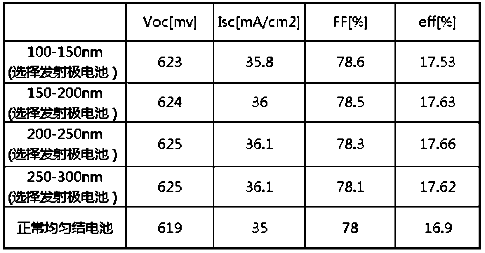

Embodiment 1

[0011] Step 1: the removal of the surface energy damage layer, the step is to put the polysilicon wafer in a sodium hydroxide solution with a mass concentration of 20% at 85-90 ° C for 80-100 seconds, and then wash it by bubbling in deionized water for 200 seconds, and then Heat and wash in 1# and 2# cleaning solution for 360s respectively. Or other conventional corrosion and cleaning methods are also available.

[0012] Step 2: The heavy doping step is to use the conventional tubular diffusion method on the cleaned and dried silicon wafer at a temperature of 850-950°C, using phosphorus oxychloride as the phosphorus diffusion source, and simultaneously injecting a volume ratio of 14:1 nitrogen and oxygen mixed gas, the diffusion time is 10-30min, the diffusion resistance is 10-30Ω / □, and then soaked in HF acid solution with 1-5% mass concentration at room temperature for 20-200s to remove silicon Surface PSG.

[0013] Step 3: growing or forming a dielectric layer or a mask l...

Embodiment 2

[0021] Step 1 and Step 2 are the same as above.

[0022] Step 3: said growing or forming a dielectric layer or a mask layer on the surface of the silicon wafer, such as using MOCVD to deposit a ZnO film, the step is to deposit a 50-300nm thick ZnO film on the surface of the silicon wafer by metal organic chemical vapor deposition. The zinc-containing DPM complex Zn(DPM)2 was used as the precursor of zinc, and the deposition time was 15-100min in the pressure range of 10-50 Torr and the temperature range of 400-600 °C.

[0023] Step 4: The step of retaining the mask layer under the electrode grid line area by the screen printing slurry etching method is: using screen printing to print a layer of corrosive slurry with a concentration of 10-25% ammonium bifluoride on the ZnO thin layer, Stand still for 400-1000s, so that the slurry fully etches away the ZnO thin layer in the non-electrode grid line area, and keep the ZnO under the electrode grid line area as a mask layer.

[002...

Embodiment 3

[0027] Step 1 and Step 2 are the same as above.

[0028] Step 3: growing or forming a dielectric layer or a mask layer on the surface of the silicon wafer, such as growing a SiNx mask layer on the surface of the silicon wafer by using PECVD technology, the step is to grow a 200-300nm SiNx mask layer on the surface of the silicon wafer by using PECVD technology film layer. SiH 4 The flow rate is 600-700sccm, NH 3 The flow rate is 1400-1500sccm, the working pressure is 0.1-0.3mbar, the process temperature is 300-500℃, the discharge frequency is 2450MHz, the discharge power is 2000-3500w, and the discharge time is 450-900s.

[0029] Step 4: Using inkjet printing technology, spray corrosive slurry with a concentration of 10-25% ammonium bifluoride on the non-electrode grid line area, and let it stand for 500-1200s, so that the slurry can fully corrode the SiNx thin film in the non-electrode grid line area. Layer, keep the SiNx under the electrode grid line area as a mask layer;...


PUM

PropertyMeasurementUnit
sizeaaaaaaaaaa

Abstract

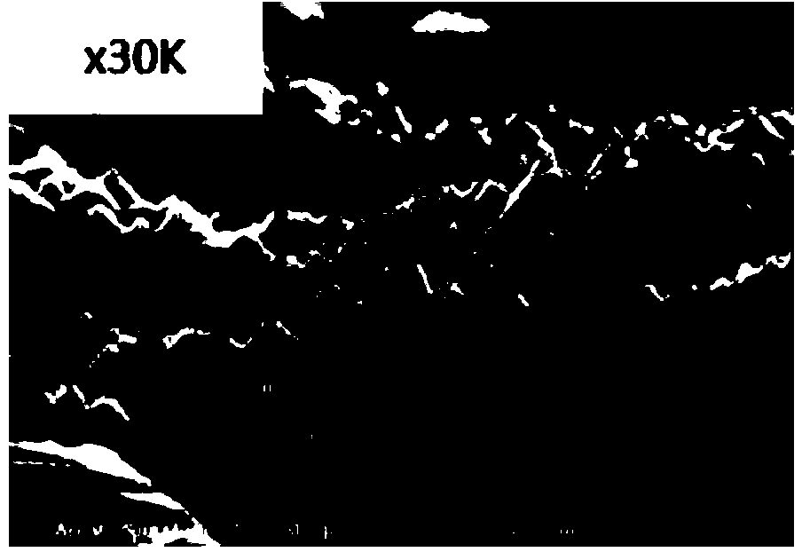
The invention discloses a preparation method for a polycrystal / monocrystal-like solar cell selective emitting electrode structure. The preparation method for the polycrystal / monocrystal-like solar cell selective emitting electrode structure comprises the following steps: (1) chemically removing a surface energy affected layer; (2) carrying out heavy doping by the one-time diffusion technology to form a PN junction; (3) growing or forming a dielectric layer or a mask layer on the surface of a silicon wafer; (4) corroding the dielectric layer of a non-electrode grid line area with a chemical corrosion method, and keeping the mask layer under an electrode grid line area; (5) etching a pyramid matte structure of 100-300nm in the non-electrode grid line area by reactive ion etching (RIE), and meanwhile, forming a shallow doped area in one time; and (6) removing a surface affected layer formed by RIE and a lower mask layer under the electrode grid line area with a wet chemistry method to obtain the selective emitting electrode structure. According to the preparation method for the polycrystal / monocrystal-like solar cell selective emitting electrode structure, which is disclosed by the invention, the light doping and the heavy doping required by the selective emitting electrode polycrystal / monocrystal-like solar cell and a low-reflectivity nanoscale surface texture can be finished by one-time diffusion combined with the RIE technology, the process path is simplified, the conversion efficiency is high, and the preparation method for the polycrystal / monocrystal-like solar cell selective emitting electrode structure is suitable for industrial volume production.

Description

Technical field: [0001] The invention relates to a method for preparing a crystalline silicon solar cell, in particular to a method for preparing a selective emitter structure of a polycrystalline / single crystal silicon solar cell. Background technique: [0002] The texturing process of polycrystalline silicon solar cells has always been using HF / HNO3 acid etching system, and the reflectivity of texturing is about 20%, which has gradually become the bottleneck process for the development of polycrystalline silicon cells; With the transformation of raw materials, the quality of polycrystalline silicon wafers is similar to that of monocrystalline silicon wafers. However, because the grain size and the number of grain boundaries are uneven due to the limitation of the drawing process, they cannot be precisely controlled, resulting in difficulties in the texturing process of quasi-single crystals. The RIE (Reactive Ion Etching) process uses SF 6 and O 2 and Cl 2 The advanced...

Claims


Application Information

Patent Timeline
Patent Type & Authority Applications(China)
IPC IPC(8): H01L31/18
CPCH01L31/022425H01L31/1804Y02E10/547Y02P70/50
Inventor 王丽春赵彦黄海冰吕俊王艾华赵建华
Owner CHINA SUNERGY CO LTD
Learn More