

Method capable of improving conversion efficiency of crystalline silicon solar cell
A solar cell and conversion efficiency technology, applied in circuits, photovoltaic power generation, electrical components, etc., can solve problems such as difficult feasibility and complex process, and achieve the effect of good feasibility, simple and easy process, and good effect.
- Summary
- Abstract
- Description
- Claims
- Application Information
AI Technical Summary
Problems solved by technology
Method used
Image

Examples
Embodiment 1
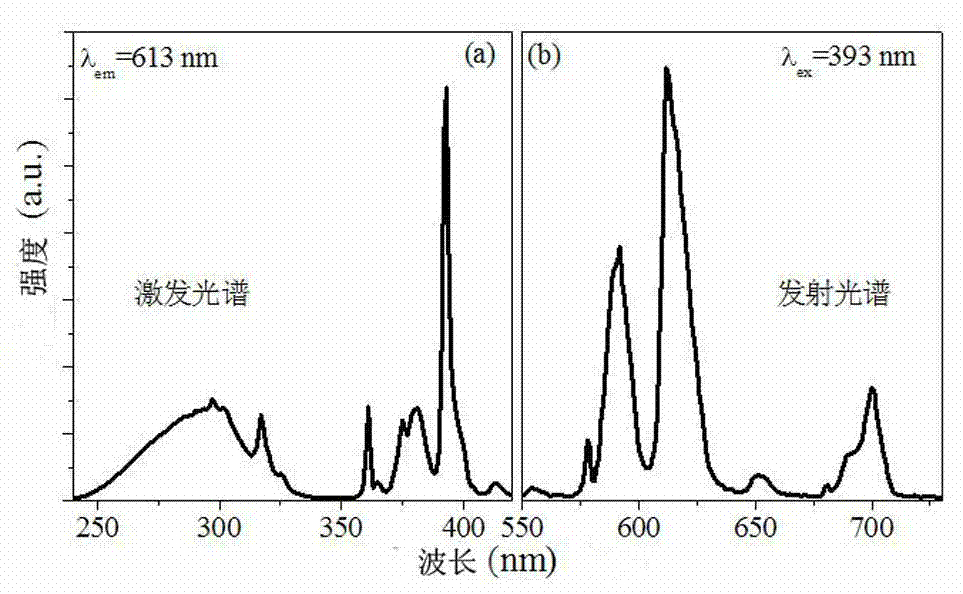
[0023] Select 156 single crystal silicon wafers, through texturing of silicon wafers (existing process), diffusion PN junction (existing process), etching and cleaning (existing process), PECVD Si plating 3 N 4 Anti-reflection coating (existing technology), film thickness 75nm, refractive index 2.0. Subsequent rare earth Eu 3+ Ion implantation, implantation parameters: implantation energy 70KeV, implantation dose 2×10 15 cm -2 . After the implantation is completed, the silicon wafer is annealed in a high-temperature furnace at 800 °C for 60 min in a nitrogen atmosphere, and then taken out and cooled to room temperature. Fluorescence spectrum test is carried out on the sample, and the attached figure 1 excitation and emission spectra. Finally, the samples are made of electrodes by screen printing (existing process) and sintered (existing process) to form a finished crystalline silicon battery with light wave conversion characteristics, and the electrical performance chara...
Embodiment 2
[0024] Example 2: Select 156 polycrystalline silicon wafers, through texturing the silicon wafers, diffusing to make PN junctions, etching and cleaning, and PECVD Si plating 3 N 4 Anti-reflection coating with a film thickness of 80 nm and a refractive index of 2.05. Subsequent rare earth Eu 3+ Ion implantation, implantation parameters: implantation energy 80KeV, implantation dose 1×10 15 cm -2 . After the implantation is completed, the silicon wafer is annealed in a high-temperature furnace at 800 °C for 30 min in a nitrogen atmosphere, and then taken out and cooled to room temperature. Fluorescence spectrum test is carried out on the sample, and the attached figure 1 excitation and emission spectra. Finally, the samples were screen-printed to form electrodes and sintered to form a finished crystalline silicon cell with light-wave conversion characteristics, and the electrical performance characteristics of the battery were tested. Compared with the existing ordinary cry...
Embodiment 3
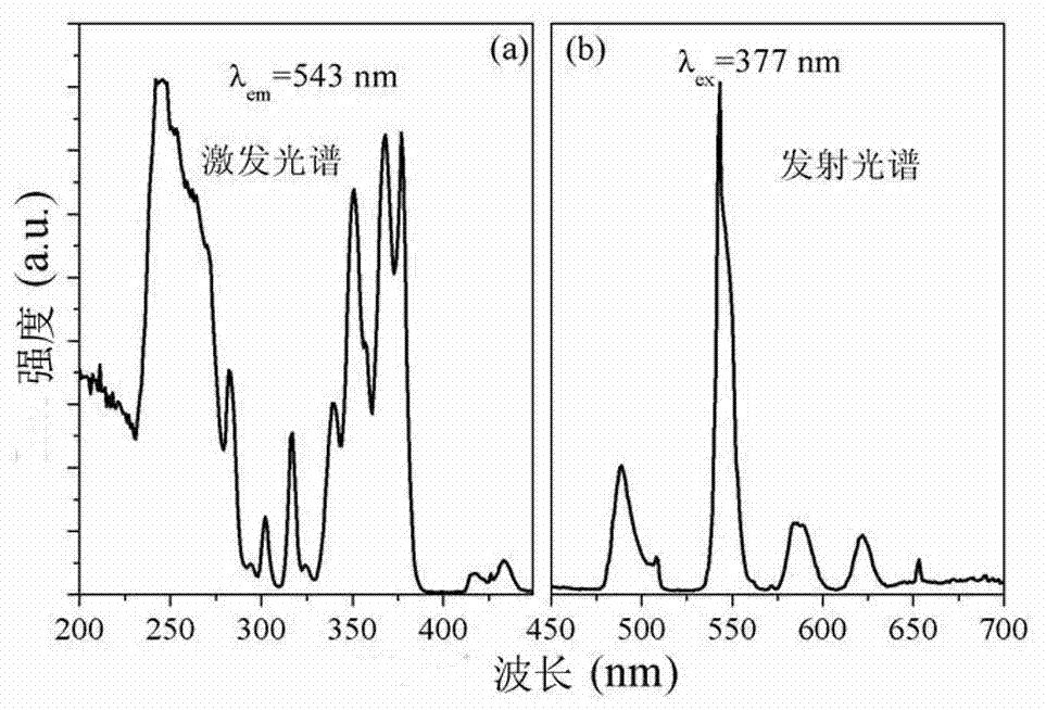
[0025] Example 3: Select 156 single crystal silicon wafers, through texturing the silicon wafers, making PN junctions by diffusion, etching and cleaning, and Si plating by PECVD 3 N 4 Anti-reflection coating with a film thickness of 90 nm and a refractive index of 2.1. Subsequent rare earth Tb in the anti-reflection coating 3+ Ion implantation, implantation parameters: implantation energy 100KeV, implantation dose 1×10 15 cm -2 . After the implantation is completed, the silicon wafer is annealed in a high-temperature furnace at 1000 °C for 30 min in a nitrogen atmosphere, and then taken out and cooled to room temperature. Fluorescence spectrum test is carried out on the sample, and the attached figure 2 excitation and emission spectra. Finally, the samples were screen-printed to form electrodes and sintered to form a finished crystalline silicon cell with light-wave conversion characteristics, and the electrical performance characteristics of the battery were tested. Co...
PUM
| Property | Measurement | Unit |
|---|---|---|
| Thickness | aaaaa | aaaaa |
Abstract
Description
Claims
Application Information