Pulsed laser deposition and molecular beam epitaxy combined coating device and application thereof

A technology of pulsed laser deposition and molecular beam epitaxy, which is applied in the fields of solar cells, laser diodes, photodetectors, light-emitting diodes, manufacturing thin film epitaxy and thin film devices, can solve problems such as limiting promotion and application scope, and achieves reduction of production costs, The effect of suppressing interface reactions and saving equipment procurement costs

Active Publication Date: 2014-08-20
广州市艾佛光通科技有限公司
View PDF3 Cites 6 Cited by
  • Summary
  • Abstract
  • Description
  • Claims
  • Application Information

AI Technical Summary

Problems solved by technology

This shortcoming of PLD seriously limits its promotion and application range.

Method used


Image

  • Pulsed laser deposition and molecular beam epitaxy combined coating device and application thereof
  • Pulsed laser deposition and molecular beam epitaxy combined coating device and application thereof
  • Pulsed laser deposition and molecular beam epitaxy combined coating device and application thereof

Examples


Embodiment 1

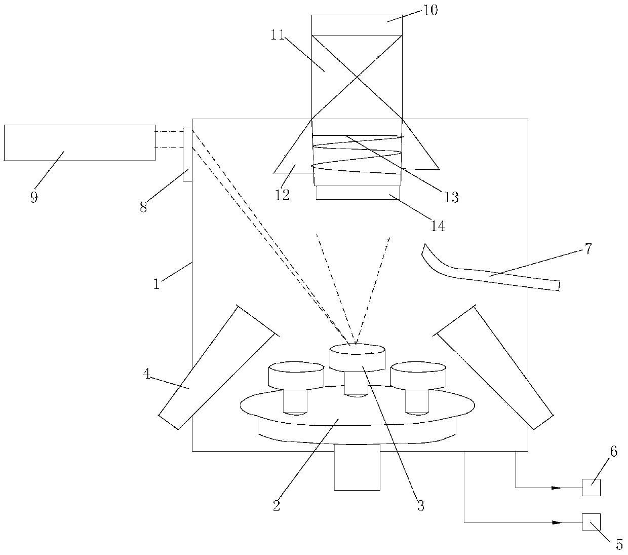
[0051] Please refer to figure 1 , A coating equipment combined with pulsed laser deposition and molecular beam epitaxy, which includes a growth chamber cavity 1;

[0052] A base 2 is provided at the center position under the growth chamber cavity 1, on the base 2 there are 1-6 evenly arranged turntables 3 for placing targets, the base 2 and the turntable 3 are respectively The driving mechanism drives the rotation, so that the target can revolve with the base 2 and rotate with the turntable 3;

[0053] A number of evenly distributed MBE evaporation sources 4 are also provided on the lower side wall of the growth chamber cavity 1;

[0054] Valves respectively connected to the mechanical pump 5 and the molecular pump 6 are provided on the lower side wall or the bottom wall of the growth chamber cavity 1, so that the mechanical pump 5 and the molecular pump 6 can vacuum the growth chamber;

[0055] An auxiliary gas pipe 7 and an RF accessory are provided at the middle and lower positions...

Embodiment 2

[0061] The method of preparing non-polar GaN-based LED epitaxial wafers by using a coating equipment combined with pulsed laser deposition and molecular beam epitaxy is as follows:

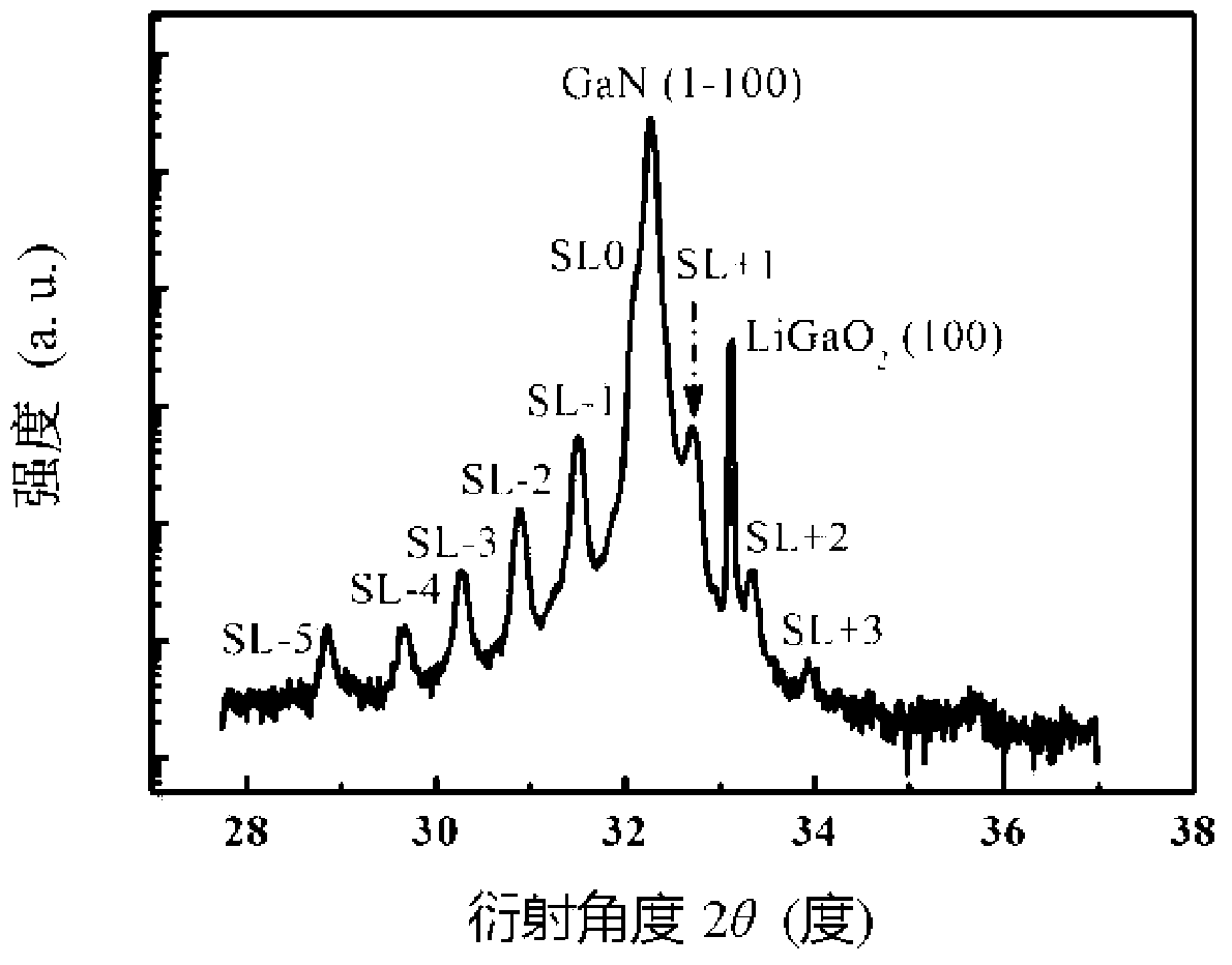
[0062] 1) Selection of the substrate and its crystal orientation: using LiGaO 2 The substrate, with the (100) plane deviating 0.2° from the (110) direction as the epitaxial plane, the crystal epitaxial orientation relationship is: the (1-100) plane of GaN is parallel to LiGaO 2 的(100)face.

[0063] 2) Polishing, cleaning and annealing the surface of the substrate;

[0064] The polishing treatment is specifically: firstly, LiGaO 2 The surface of the substrate is polished with diamond slurry, and the surface of the substrate is observed with an optical microscope until there are no scratches, and then chemical mechanical polishing is used for polishing;

[0065] The cleaning treatment is specifically: LiGaO 2 The substrate is placed in deionized water and ultrasonically cleaned for 3 minutes at room temperat...

Embodiment 3

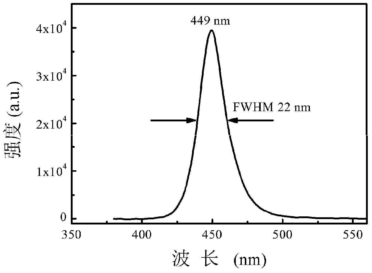
[0078] The pulsed laser deposition and molecular beam epitaxy combined coating equipment described in Example 1 is used to prepare a GaN thin film grown on a lithium gallate substrate, and the GaN thin film is used to prepare LEDs: Si-doped n-type silicon-doped GaN and In are sequentially epitaxially grown on the GaN film on the x Ga1-xN multiple quantum well layer, Mg-doped p-type magnesium-doped GaN layer, and finally electron beam evaporation to form an ohmic contact. The thickness of the n-type GaN of the GaN-based LED device prepared on the lithium gallate substrate is about 4.5μm, and the carrier concentration is 1.7×10 19 cm -3 ; In x Ga 1-x The thickness of the N / GaN multiple quantum well layer is about 150nm, and the number of periods is 10, where In x Ga 1-x The N-well layer is 3nm, the GaN barrier layer is 12nm, the thickness of the p-type Mg-doped GaN layer is about 300nm, and the carrier concentration is 4.9×10 17 cm -3 . At a working current of 20mA, the light outp...


PUM

PropertyMeasurementUnit
thicknessaaaaaaaaaa
thicknessaaaaaaaaaa
thicknessaaaaaaaaaa

Abstract

The invention discloses a pulsed laser deposition and molecular beam epitaxy combined coating device and application thereof. A target material tray capable of conducting revolution and rotation is added to the middle area of an MBE evaporation source, and a target material required by PLD coating is placed; a high-performance solid laser device is added, and meanwhile a quartz window is added to an appropriate position of a cavity of an MBE growth chamber and high-energy lasers with the wave length of 150 nm to 355 nm are introduced for evaporation of the target material. The coating device is a PLD and MBE combined body and has the functions and advantages of a PLD and an MBE at the same time; the coating device can be used as the PLD or the MBE individually and can also be used as the combination of the PLD and the MBE; the coating device can be used for epitaxial growth of a thin film and manufacturing of thin film devices, especially for solar cells, LEDs and LDs of a quantum well structure. Compared with the prior art, the coating device has the advantages of being simple in growth process, low in manufacturing cost and wide in application range.

Description

Technical field [0001] The invention relates to a coating equipment for pulse laser deposition (PLD) combined with molecular beam epitaxy (MBE) and its application. It is specifically used to manufacture thin film epitaxy and thin film devices, especially solar cells, light emitting diodes (LED), and laser diodes ( LD), photodetector. Background technique [0002] With the rapid population expansion and the development and progress of science and technology, mankind's demand for energy continues to increase. However, many energy sources such as oil and coal are non-renewable resources, and the lack of energy has become a huge obstacle to human development and progress. How to use existing energy sources more effectively and achieve sustainable development is a major problem faced by all mankind. Especially at present, in the context of increasingly severe global warming, the world is still facing important issues of saving energy and reducing greenhouse gas emissions. Therefor...

Claims


Application Information

Patent Timeline
Patent Type & Authority Applications(China)
IPC IPC(8): H01L21/20H01L21/203H01L33/00
CPCC23C14/28C30B25/02H01L33/0066H01L33/0075
Inventor 李国强
Owner 广州市艾佛光通科技有限公司
Why Eureka
Try Eureka