Protected thermoelectric element, thermoelectric device comprising same and forming method thereof
A thermoelectric element and protected technology, which is applied in the manufacture/processing of thermoelectric device components and thermoelectric devices, etc., can solve problems such as large differences in thermal expansion coefficients, reduced coating packaging effects, and imperfect connections
- Summary
- Abstract
- Description
- Claims
- Application Information
AI Technical Summary
Problems solved by technology
Method used
Image
Examples
preparation example Construction
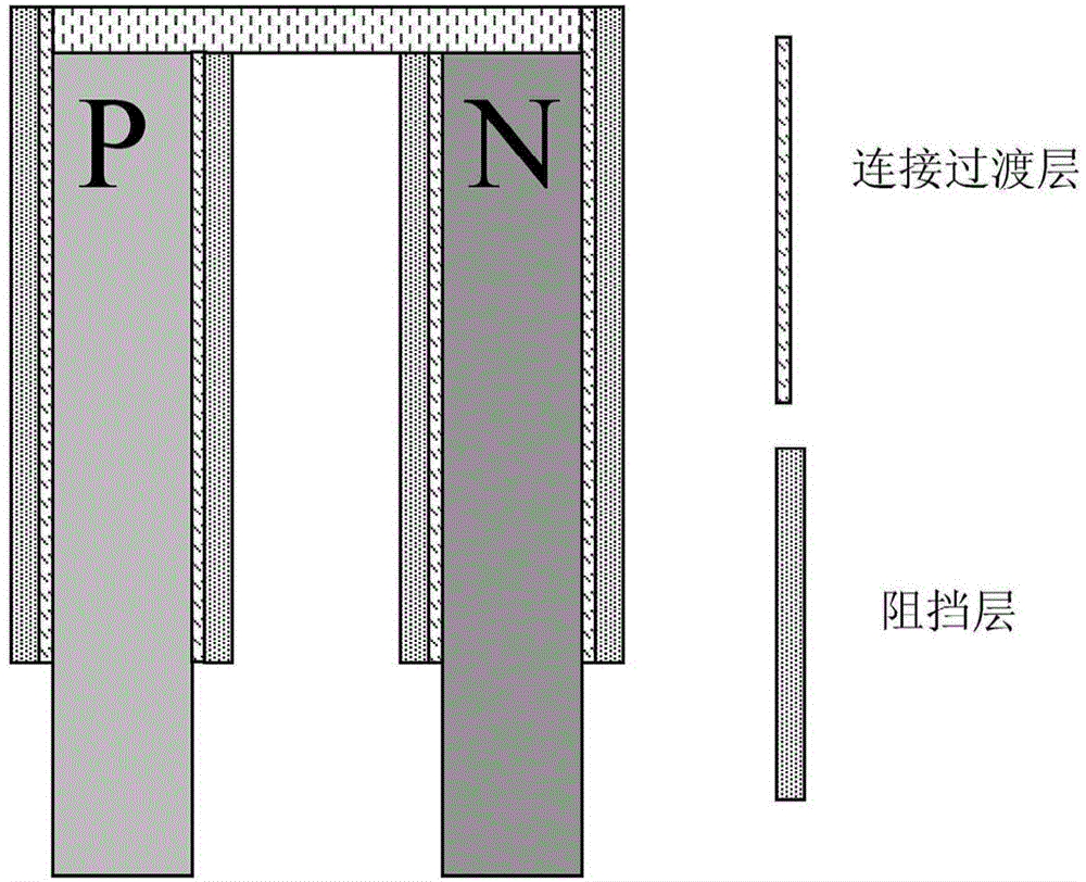
[0041] To this end, the present invention relates to a thermoelectric element with a multilayer structure protective layer and a method for preparing the same. The basic composition of thermoelectric elements with protective coating is skutterudite / (connecting transition layer structure / barrier layer structure) n (n=1~10). The skutterudite material can be based on CoSb 3 Base or Y x Fe y co (4-y) Sb 12 The skutterudite compound is the basic composition. On this basis, various skutterudite compounds are prepared by doping, filling, doping and filling or compounding. The materials connecting the transition layer structure include Mg, Al, Si, Ti, Various simple substances of V, Cr, Mn, Ni, Zn, Y, Zr, Nb, Mo, Pd, Sb, Ta, W or binary or multi-component alloys composed of two or more of the aforementioned components, Or their intermetallic compounds, and titanium alloys, NiCr alloys, and NiAl alloys containing other components, or one or more alloys formed by these elemental, ...
Embodiment 1
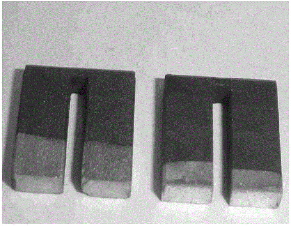
[0093] n-CoSb 3 The nominal composition of the matrix-filled skutterudite material is Yb 0.3 co 4 Sb 12 , process the sintered block material into 3×5×12mm 3 cuboid sample. Firstly, an Al-Cr alloy layer of about 5 μm is formed on the surrounding surface of the material by electron beam evaporation. The process parameters of electron beam evaporation are: arc voltage 4-8kV, working current 80-120mA, evaporation rate is about 38nm / min. On the Al-Cr layer, a layer of TiAlN coating with a thickness of about 3 μm was prepared by magnetron sputtering, the flow rate of nitrogen gas was 9ml / min, the flow rate of argon gas was 20ml / min, the deposition temperature was 240°C, and the sputtering power was 50W. The coated and encapsulated materials are placed in air at 550°C, kept warm for 1 hour, then taken out directly, and placed in air at room temperature to cool down to room temperature. This process acts as an accelerated thermal shock cycle. After 100 accelerated thermal sho...
Embodiment 2
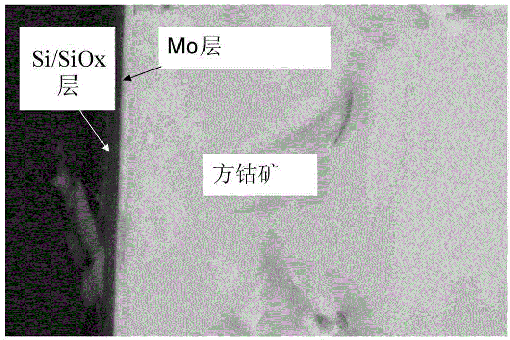
[0095] p-CoSb 3 The nominal composition of the matrix-filled skutterudite material is CeFe 4 Sb 12 , process the sintered block material into 3×5×12mm 3 cuboid sample. First, a Ti layer of about 2 μm is formed on the surrounding surface of the material by magnetron sputtering. The diameter of the Ti target is 80mm, the thickness is 5mm, the sputtering gas is high-purity argon (the purity of Ar is 99.999%), and the flow rate of argon is 15mL / min. During coating, the back vacuum of the system is 10Pa, and the working air pressure is 0.2Pa. The sample temperature is normal temperature (20° C.), the sputtering power is 60 W, and the film deposition rate is about 20 nm / min. Then, a nickel-chromium-aluminum-yttrium (NiCrAlY) layer of about 3 μm is formed on the Ti layer by magnetron sputtering, the sputtering power is 2.1-2.4 kW, the argon gas pressure is 0.2 Pa, and the substrate temperature is 250° C. Finally, a layer of chromium silicide with a thickness of 2 μm was evapora...
PUM
| Property | Measurement | Unit |
|---|---|---|
| thickness | aaaaa | aaaaa |
| thickness | aaaaa | aaaaa |
| thickness | aaaaa | aaaaa |
Abstract
Description
Claims
Application Information


