Inverted-structure CdTe nanocrystalline heterojunction high-efficiency solar cell processed by solution method, and preparation method of solar cell

A technology of solar cells and inverted structures, which is applied in nanotechnology, nanotechnology, nanotechnology, etc. for materials and surface science, and can solve the problems of difficult device stability, unfavorable carrier separation and transmission, and reduced light absorption. Efficiency and other issues, to improve battery performance, reduce roughness, improve the effect of the interface

Inactive Publication Date: 2015-04-08
SOUTH CHINA UNIV OF TECH
View PDF2 Cites 12 Cited by
  • Summary
  • Abstract
  • Description
  • Claims
  • Application Information

AI Technical Summary

Problems solved by technology

[0005] In 2010, Anderson (J.D.Olson, Y.W.Rodriguez, L.D.Yang, G.B.Alers, S.A.Carter, Appl.Phys.Lett., 2010, 96, 242103.) research group developed non-aluminum metal electrodes and studied CdTe, CdSe layers The effect of thickness on device performance, found that by increasing the thickness of the CdTe layer, better energy conversion efficiency can be obtained, but the conversion efficiency of the best device is only 2.6%
This kind of active layer is on the ITO substrate, and the n-type layer is the outermost layer. There are certain problems: the active layer CdTe is directly spin-coated on the ITO, and the light is incident from one side of the ITO, so the p-n junct

Method used


Image

  • Inverted-structure CdTe nanocrystalline heterojunction high-efficiency solar cell processed by solution method, and preparation method of solar cell
  • Inverted-structure CdTe nanocrystalline heterojunction high-efficiency solar cell processed by solution method, and preparation method of solar cell
  • Inverted-structure CdTe nanocrystalline heterojunction high-efficiency solar cell processed by solution method, and preparation method of solar cell

Examples


preparation example Construction

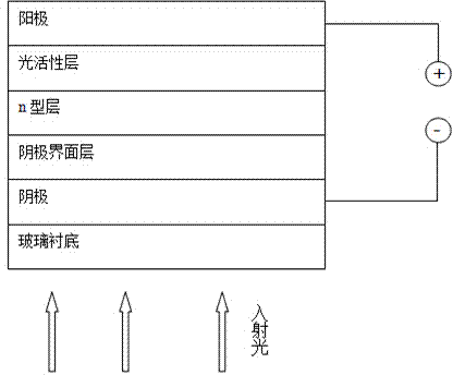
[0048] (3) Preparation of the cathode interface layer: place the ITO sheet on a homogenizer (KW-4A type), drop the ZnO sol prepared in step (2), spin-coat at high speed (3000rpm, time 20s), scrape off The ZnO layer at the cathode position was placed on a heating platform, firstly heat-treated at 200°C for 10 minutes, then heated at 400°C for 10 minutes, cooled to room temperature, placed in acetone and isopropanol and ultrasonicated for 10 minutes (ultrasonic power 1000W), blown with a nitrogen gun Dry to obtain a cathode interface layer with a thickness of 40 nm.

[0049] (4) Preparation of n-type layer:

[0050] ① Preparation of CdSe nanocrystals: Weigh cadmium myristate (1.6mmol, 906mg), trioctylphosphine oxide 2.35g, myristic acid (myristic acid, C 13 h 26COOH, 92mg) was added into a 50ml three-necked bottle (the mouth of the bottle was equipped with a thermometer, a condenser tube, and an air guide tube), and heated to 240°C under nitrogen protection. At this time, the ...

Embodiment 1

[0068] Effect of different CdSe layer thicknesses on CdTe nanocrystalline cells.

[0069] CdSe nanocrystalline layers with a thickness of 30nm, 60nm, 90nm, 120nm, and 150nm were selected as the n-type layer, ZnO was set at 40nm, CdTe layer was set at 500nm, and CdCl 2 The sintering temperature was set at 340°C to prepare CdTe nanocrystalline solar cells. Table 2 compares the device results for different CdSe layer thicknesses.

[0070] Table 2 Effect of CdSe layer thickness on performance of CdTe nanocrystalline solar cells

[0071]

[0072] Table 2 compares the effect of CdSe layer thickness on device performance. The results of multiple experiments show that when the thickness of the CdSe nanocrystalline window layer is 60-90nm, the open-circuit voltage of the device rises significantly, and the performance is obviously improved. Under this thickness, it not only ensures that enough light can pass through the CdSe layer to reach the photoactive area, but also ensures t...

Embodiment 2

[0074] Effect of different CdTe layer thicknesses on CdTe nanocrystalline cells.

[0075] Using a specific implementation method, the inverted structure is prepared as an ITO / ZnO / CdSe / CdTe / Au inverted structure device, wherein the thickness of the CdSe layer is 60nm, the thickness of the CdTe layer is respectively 200nm, 300nm, 400nm, 500nm, 600nm, and 700nm, and the thickness of the ZnO layer is 40nm, CdCl 2 The sintering temperature was 340°C. Detect the short-circuit current density (mA / cm2) of each device 2 ), open circuit voltage (V), fill factor (%), energy conversion efficiency (%). Table 3 compares the results for devices with different CdTe layer thicknesses:

[0076] Table 3 Effect of CdTe layer thickness on performance of CdTe nanocrystalline solar cells

[0077]

[0078] It can be seen from Table 3 that when the thickness of the CdTe layer is about 500nm, the energy conversion efficiency is the highest. Under this thickness, the active layer with a certain t...


PUM

PropertyMeasurementUnit
Thicknessaaaaaaaaaa
Thicknessaaaaaaaaaa
Thicknessaaaaaaaaaa

Abstract

The invention provides an inverted-structure CdTe nanocrystalline heterojunction high-efficiency solar cell processed by a solution method, and a preparation method of the solar cell. The solar cell is formed by sequentially overlapping a glass substrate, a cathode, a cathode interface layer, an n-type layer, a photoactive layer and an anode together from bottom up, wherein the thickness of the photoactive layer is 100-700 nm; the photoactive layer consists of one or more CdTe nanocrystalline layers; and the n-type layer is a CdSe film. According to the invention, energy conversion rate of the CdTe- CdSe full-inorganic nanocrystalline heterojunction solar cell is greatly increased; open-circuit voltage and a fill factor of the solar cell are increased; and the service life of the solar cell is greatly prolonged. The method is simple in preparation technology; the main process can be completed by solution processing in a common fuming cupboard; comparatively low temperature heat treatment is employed and the preparation cost is greatly lowered.

Description

technical field [0001] The invention belongs to the field of photoelectric devices, in particular to an inverted structure CdTe nanocrystalline heterojunction high-efficiency solar cell processed by a solution method and a preparation method thereof. Background technique [0002] Since the 21st century, fossil energy has been on the verge of exhaustion after decades of large-scale exploitation and use. Since the industrial revolution, the greenhouse effect has caused the average temperature of the earth to rise by 0.3-0.6°C, and the sea level has risen by 10-25cm. The main component of the greenhouse gas is carbon dioxide, 80% of which is produced by the consumption of fossil fuels. It can be seen that human beings are facing the double crises of energy shortage and environmental degradation. The development of an efficient and clean energy source is an urgent problem for mankind today. The development of solar energy is an inevitable trend of today's energy mining, becau...

Claims


Application Information

Patent Timeline
IPC IPC(8): H01L31/109H01L31/0296H01L31/18H01L31/0224
CPCB82Y30/00B82Y40/00H01L31/022425H01L31/0296H01L31/035281H01L31/109H01L31/1828Y02E10/543Y02P70/50
Inventor 覃东欢卢宽宽刘涵谢雅吴荣方
Owner SOUTH CHINA UNIV OF TECH
Why Eureka
Try Eureka