
Organic/gallium nitride heterogeneous p-n junction ultraviolet light detector and preparing method thereof

A technology of ultraviolet light and detectors, which is applied in the fields of organic semiconductor devices, semiconductor/solid-state device manufacturing, photovoltaic power generation, etc., can solve the problems of high manufacturing cost of ultraviolet light detectors, inability to be widely used, high difficulty in doping technology, etc., to achieve Excellent device performance, low price, and excellent photoelectric performance

Active Publication Date: 2015-04-29
SUZHOU INST OF NANO TECH & NANO BIONICS CHINESE ACEDEMY OF SCI
View PDF4 Cites 9 Cited by
  • Summary
  • Abstract
  • Description
  • Claims
  • Application Information

AI Technical Summary

Problems solved by technology

However, although the photoelectric properties of single crystal thin film devices are excellent, there are still many problems to be solved in this kind of high-quality single crystal semiconductor thin film, such as the required equipment is expensive, and the growth and doping technology is difficult. These factors make single crystal The manufacturing cost of semiconductor thin-film ultraviolet light detectors is still very high, and cannot be widely used

Method used


Image

  • Organic/gallium nitride heterogeneous p-n junction ultraviolet light detector and preparing method thereof
  • Organic/gallium nitride heterogeneous p-n junction ultraviolet light detector and preparing method thereof
  • Organic/gallium nitride heterogeneous p-n junction ultraviolet light detector and preparing method thereof

Examples


Embodiment 1

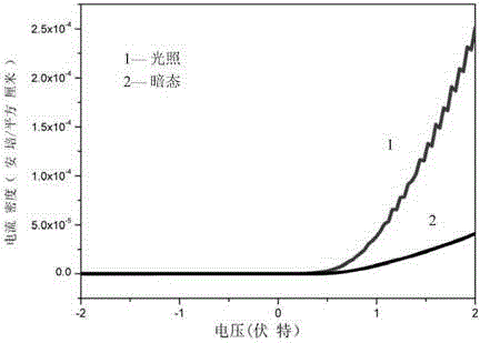
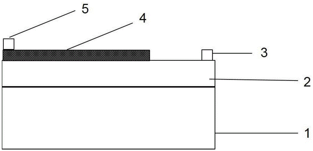
[0042] GaN films were grown by metal-organic vapor deposition, and NH 3 As a nitrogen source, trimethylgallium (TMGa) or triethylgallium (TEGa) is used as a gallium source, and the reaction temperature is higher than 900 degrees Celsius, and epitaxially grows a GaN film on a sapphire substrate. Afterwards, GaN was ultrasonically cleaned with acetone and ethanol, rinsed with deionized water and dried. The side electrodes are prepared by evaporating metal Ti / Al / Ni / Au on the GaN substrate with a specific thickness of 20nm / 120nm / 70nm / 100nm and annealing at 200°C / 585°C / 600°C / 885°C respectively . GaN is used as the working electrode, PT wire is used as the side electrode and the counter electrode, placed in the electrolyte (0.05mM pyrrole + 0.1mM sodium perchlorate aqueous solution), and the electrochemical deposition is performed by chronopotential method, and the current density is 0.1mA / cm 2 , the deposition time is 1.5h, so as to obtain the organic / GaN composite heterojunction...

Embodiment 2

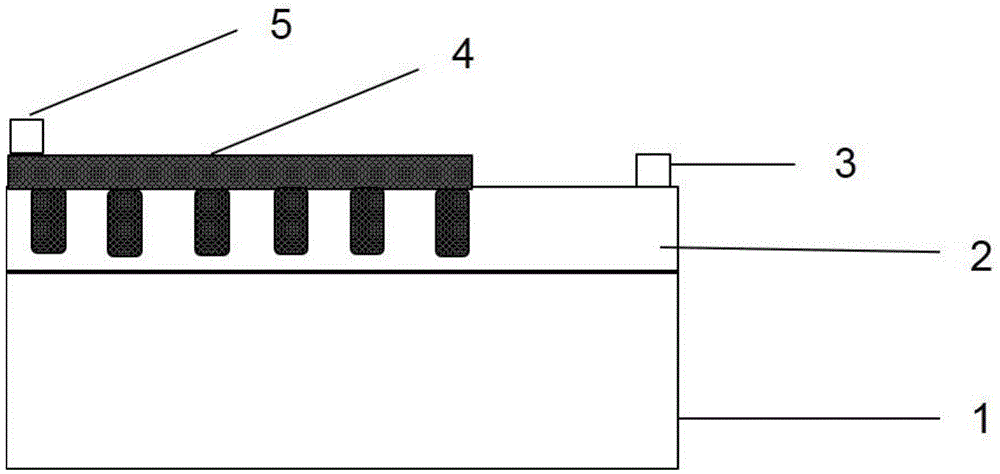
[0044] GaN films were grown by metal-organic vapor deposition, and NH 3As a nitrogen source, trimethylgallium (TMGa) or triethylgallium (TEGa) is used as a gallium source, and the reaction temperature is higher than 900 degrees Celsius, and epitaxially grows a GaN film on a sapphire substrate. The grown GaN thin film is etched by dry etching to obtain porous GaN, and then ultrasonically cleaned with acetone and ethanol, rinsed with deionized water and dried. The side electrodes are prepared by evaporating metal Ti / Al / Ni / Au on the GaN substrate with a specific thickness of 20nm / 120nm / 70nm / 100nm and annealing at 200°C / 585°C / 600°C / 885°C respectively . GaN is used as the working electrode, PT wire is used as the side electrode and the counter electrode, placed in the electrolyte (0.05mM pyrrole + 0.1mM sodium perchlorate aqueous solution), and the electrochemical deposition is performed by chronopotential method, and the current density is 0.1mA / cm 2 , the deposition time is 1.5...

Embodiment 3

[0046] GaN films were epitaxially grown on silicon carbide substrates by gas source molecular beam epitaxy, and the gas source was N 2 . Afterwards, the epitaxially grown GaN film was ultrasonically cleaned with acetone and ethanol, rinsed with deionized water and dried. Evaporated metal by electron beam on GaN substrate: Ni / Au, the thickness is 20 / 120nm respectively,

[0047] And the side electrode is prepared by high temperature annealing method at 600°C / 885°C. Using GaN as the working electrode, PT wire as the side electrode and the counter electrode, placed in the electrolyte (0.2M aniline + 0.5M sulfuric acid aqueous solution), the electrochemical deposition was carried out by chronoamperometry, where the voltage was 8V, and the deposition time was 2h. An organic / GaN composite heterojunction structure is obtained. Finally, silver paste is placed on the organic layer and annealed at 110 degrees Celsius for 20 minutes as an electrode material. The structure and performa...


PUM

PropertyMeasurementUnit
Thicknessaaaaaaaaaa

Abstract

The invention discloses an organic / gallium nitride heterogeneous p-n junction ultraviolet light detector and a preparing method thereof. The detector comprises an organic / GaN heterogeneous p-n junction mainly formed by a GaN layer and an organic layer which are arranged in an overlapped way in a set direction, wherein a first electrode and a second electrode are respectively connected to the GaN layer and the organic layer. The preparing method comprises the following steps: after growing the GaN layer on a substrate by an extension growing technology, forming the first electrode on the GaN layer by a metal material, covering the organic layer on the GaN layer, and then arranging the second electrode on the organic layer. The ultraviolet light detector is made of a wide-band gap semiconductor material and an organic semiconductor material together and fully utilizes the advantages of the inorganic semiconductor material and the organic material. Meanwhile, the device is simple in preparing technology and easy to realize. The device performance can be greatly improved under the condition of effectively saving cost.

Description

technical field [0001] The invention relates to an ultraviolet photodetector and a preparation method thereof, in particular to a novel organic / GaN heterogeneous p-n junction ultraviolet photodetector and a preparation method thereof, belonging to the field of semiconductor devices. Background technique [0002] Ultraviolet light detector is a kind of photodetector widely used in military and civilian fields. As a third-generation semiconductor, gallium nitride (GaN) and its series of materials (indium nitride, aluminum nitride, gallium nitride) are known for their wide range, wide spectral range (covering the entire range from ultraviolet to infrared), and It has good high temperature and corrosion resistance, and has great application value in the fields of optoelectronics and microelectronics. GaN-based ultraviolet detector is a very important GaN-based optoelectronic device, which has important application value in civilian and military fields such as missile warning, u...

Claims


Application Information

Patent Timeline
IPC IPC(8): H01L51/42H01L51/46H01L51/48B82Y40/00
CPCH10K71/231H10K30/00H10K2102/00Y02E10/549
Inventor 潘革波胡立峰邓凤祥赵宇肖燕
Owner SUZHOU INST OF NANO TECH & NANO BIONICS CHINESE ACEDEMY OF SCI
Learn More