Organic electroluminescence device and preparation method thereof

An electroluminescent device and a luminescent technology, which are applied in the fields of electric solid-state devices, semiconductor/solid-state device manufacturing, electrical components, etc., can solve problems such as poor film-forming properties of lithium fluoride, easy formation of electronic defects, and electronic quenching

Inactive Publication Date: 2015-05-27
OCEANS KING LIGHTING SCI&TECH CO LTD +2
View PDF0 Cites 0 Cited by
  • Summary
  • Abstract
  • Description
  • Claims
  • Application Information

AI Technical Summary

Problems solved by technology

[0003] The electron injection layer of traditional organic electroluminescent devices generally uses lithium fluoride, but because the melting point of lithium fluoride is too high, a large current must be used for evaporation during evaporation, and the evaporation room of the organic evaporation room is too high , will damage other organic functional layers, and the film-forming property of lithium fluoride is poor, and it is easy to form electron defects, resulting in the quenching of electrons and reducing the recombination probability of electrons and holes

Method used


Image

  • Organic electroluminescence device and preparation method thereof
  • Organic electroluminescence device and preparation method thereof
  • Organic electroluminescence device and preparation method thereof

Examples


preparation example Construction

[0036] The preparation method of the organic electroluminescence device 100 of an embodiment, it comprises the following steps:

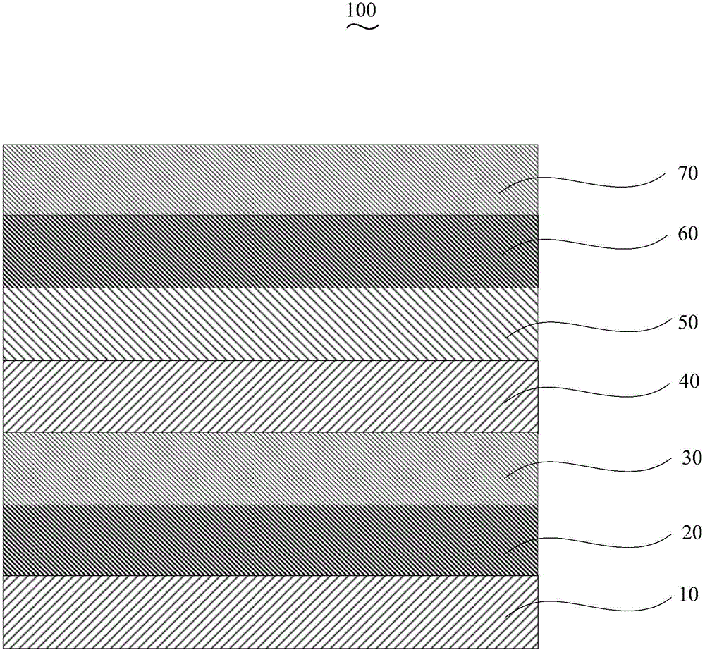
[0037] Step S110 , sequentially forming a hole injection layer 20 , a hole transport layer 30 , a light emitting layer 40 , an electron transport layer 50 and an electron injection layer 60 on the surface of the anode 10 .

[0038] The anode 10 is indium tin oxide glass (ITO), fluorine-doped tin oxide glass (FTO), aluminum-doped zinc oxide glass (AZO) or indium-doped zinc oxide glass (IZO), preferably ITO, and the thickness of the anode 10 is 50 nm to 300 nm, preferably 80 nm.

[0039] In this embodiment, before the hole injection layer 20 is formed on the surface of the anode 10, the anode 10 is pretreated. The pretreatment includes: performing photolithography on the anode 10, cutting it into the required size, using detergent, deionized Water, acetone, ethanol, and isopropanone were each ultrasonically cleaned for 15 minutes to remove organic po...

Embodiment 1

[0054] The structure ITO / MoO prepared in this embodiment 3 / NPB / Alq 3 / Bphen / Rb 2 CO 3 :UGH2 / Ca:Alq 3 / Ag organic electroluminescent device, in this embodiment and the following embodiments, " / " indicates a layer, and ":" indicates doping.

[0055] Magnetron sputtering anode on the glass substrate, the material is ITO, and then photolithography treatment, cut into the required size, followed by detergent, deionized water, acetone, ethanol, isopropanol ultrasonic 15min each, to remove the glass surface organic pollutants; after cleaning, carry out proper treatment on the conductive substrate: oxygen plasma treatment, the treatment time is 5min, the power is 30W; the thickness is 80nm, and the hole injection layer is evaporated, and the material is MoO 3 , with a thickness of 25nm; the vapor-deposited hole transport layer, the material is NPB, and the thickness is 55nm; the vapor-deposited light-emitting layer, the material is Alq 3 , with a thickness of 16nm; the vapor-dep...

Embodiment 2

[0062] The structure prepared in this example is IZO / MoO 3 / TCTA / DCJTB / TPBi / RbCl:UGH1 / Mg:Bphen / Au organic electroluminescence device.

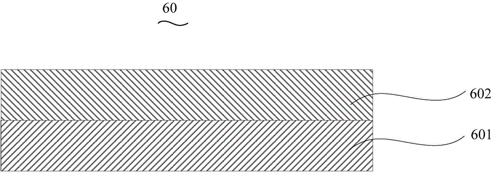
[0063] Magnetron sputtering anode on the glass substrate, the material is IZO, and then photolithography treatment, cut into the required size, followed by detergent, deionized water, ultrasonic 15min, remove the organic pollutants on the glass surface; Hole injection layer: material is MoO 3 , with a thickness of 40nm; evaporated hole transport layer: the material is TCTA, with a thickness of 45nm; evaporated luminescent layer: the selected material is DCJTB, with a thickness of 8nm; evaporated electron transport layer, the material is TPBi, with a thickness of 65nm; The injection layer includes a binary doped layer and a metal doped layer. The binary doped layer is vapor-deposited with thermal resistance. The material is RbCl:UGH1, the mass ratio of RbCl to UGH1 is 2:1, and the thickness is 50nm; A metal doped layer is prepared on the surf...


PUM


Abstract

An organic electroluminescence device comprises an anode, a hole injection layer, a hole transporting layer, a luminous layer, an electron transporting layer, an electron injection layer and a cathode which are overlapped in sequence, wherein the electron injection layer comprises a two-element-doped layer and a metal doped layer; the two-element-doped layer is made of one or more rubidium compound materials and an organosilicon small molecular material; the rubidium compound material(s) is / are one or more of rubidium carbonate, rubidium chloride, rubidium nitrate and rubidium sulfate; the energy gap of the organosilicon small molecular material is -3.5 eV to -5.5 eV; the metal doped layer is made of one or more of metal materials and one or more electron transporting materials; the work function of the metal materials is -2.0 eV to -3.5 eV; the electron transporting material(s) is / are one or more of 4,7-diphenyl-1,10-phenanthroline, 2-(4'-tert-butylphenyl)-5-(4'-biphenyl)-1,3,4-oxadiazole, 8-hydroxyquinoline aluminum, and N-aryl benzimidazole.

Description

technical field [0001] The invention relates to an organic electroluminescence device and a preparation method thereof. Background technique [0002] The luminescence principle of organic electroluminescent devices is based on the action of an external electric field, electrons are injected from the cathode to the lowest unoccupied molecular orbital (LUMO) of organic matter, and holes are injected from the anode to the highest occupied molecular orbital (HOMO) of organic matter. Electrons and holes meet, recombine, and form excitons in the light-emitting layer. Excitons migrate under the action of an electric field, transfer energy to the light-emitting material, and excite electrons to transition from the ground state to the excited state. The excited state energy is deactivated by radiation to generate photons , releasing light energy. [0003] The electron injection layer of traditional organic electroluminescent devices generally uses lithium fluoride, but because the m...

Claims


Application Information

Patent Timeline
Patent Type & Authority Applications(China)
IPC IPC(8): H01L51/50H01L51/54H01L51/56
Inventor 周明杰黄辉陈吉星王平
Owner OCEANS KING LIGHTING SCI&TECH CO LTD
Why Eureka
Try Eureka