Method for extracting semiconductor elements through photoelectrochemistry metallurgy

A photoelectrochemical and semiconductor technology, applied in the direction of optics, electrolytic process, electrolytic components, etc., can solve the problems of short process, high energy consumption and low cost

Active Publication Date: 2015-11-25
CENT SOUTH UNIV
View PDF6 Cites 9 Cited by
  • Summary
  • Abstract
  • Description
  • Claims
  • Application Information

AI Technical Summary

Problems solved by technology

[0008] The purpose of the present invention is to overcome the problems of high energy consumption and high loss rate in the traditional semiconductor element extraction process, and provide a metallurgical extraction process with short process, high recovery rate, low cost and comprehensive utilization of clean energy

Method used


Image

  • Method for extracting semiconductor elements through photoelectrochemistry metallurgy
  • Method for extracting semiconductor elements through photoelectrochemistry metallurgy
  • Method for extracting semiconductor elements through photoelectrochemistry metallurgy

Examples


Embodiment 1

[0071] Get an appropriate amount of selenium soot leaching solution and add HCl thereinto, make the [H of the leaching solution after mixing evenly + ] reached 1.0mol / L, the concentration of Se was 1.3mol / L, and the prepared leachate was added to the three-electrode system as electrolyte for subsequent use. A stainless steel plate is used as the cathode, graphite is used as the anode (the distance between the cathode and the anode is 8 mm), and a saturated calomel electrode is used as the reference electrode. Control the electrolyte temperature to 70°C,

[0072] Carry out the following experiment according to the above conditions

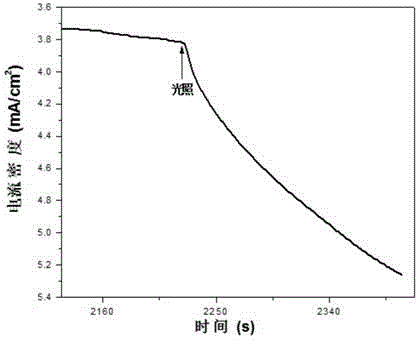
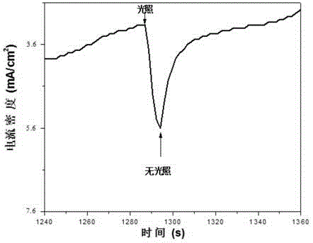
[0073] A1 uses a xenon lamp to introduce light intensity to the cathode at 100mW / cm 2 (the intensity of illumination is the intensity of the introduced cathode irradiation light on the surface of the cathode), when the cathode deposition potential is controlled to be -0.1V (vsNHE), the cell voltage is 0.9V, and the cathode reduction current densit...

Embodiment 2

[0092] Take an appropriate amount of metallurgical intermediate tellurium dioxide TeO 2 Add NaOH solution and dissolve, add the sodium sulfide solution of 0.7g / L to remove the impurity metal ion in the solution to the alkali solution that has dissolved tellurium dioxide, the prepared solution is the electrolytic solution of photoelectrochemical extraction (wherein the tellurium content is 100~120g / L, NaOH70~120g / L, Se2 , the control tank voltage is 2.5V, with 100mW / cm 2 Sunlight is used as a light source to shine vertically on the cathode through the electrolyte. Keep the cathode deposition time for 120h, then take out the cathode, clean it and cast an ingot, the purity of the refined tellurium block obtained after melting and casting is >99.9%, the energy consumption of preparing refined tellurium by this scheme is 40% lower than that of the traditional method, and the deposition efficiency is increased to The original 180% is a low-energy hydrometallurgical process.

Embodiment 3

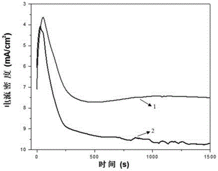
[0094] Take an appropriate amount of tellurium powder obtained by reduction with sodium sulfite, and leaching it with oxidation alkali, and the obtained leaching solution is used as an electrolyte (pH value is 12.8, concentration of tellurium is 5.1mol / L), and it is added to the three-electrode system for later use. transparent SnO 2 The conductive glass is the cathode, the thick tellurium is the anode (the distance between the cathode and the anode is 30mm), the reference electrode is a saturated calomel electrode, 50mW / cm 2 The xenon lamp is stably irradiated as the light source, and the photons pass through the transparent SnO 2 The transmission of the conductive glass reaches the surface of the cathode, the temperature of the electrolyte is controlled at 30°C, the potential of the cathode electrode is controlled at -0.3V (vsNHE), and the cell voltage is controlled at 1.7V so that the cathode current density of the reduction system is 95-110A / m 2 . After the deposition ti...


PUM

PropertyMeasurementUnit
electrical resistivityaaaaaaaaaa
pore sizeaaaaaaaaaa
strengthaaaaaaaaaa

Abstract

The invention belongs to the technical field of hydrometallurgy, and relates to a method for extracting semiconductor elements through photoelectrochemistry metallurgy, in particular to photoelectrochemistry extraction of the semiconductor elements such as tellurium, germanium, selenium, tin, antimony and bismuth. In an electrolytic deposition pool, irradiation light is led into the cathode, and a semiconductor is obtained on the cathode through photoelectrochemistry deposition, wherein an electrolyte for electrolysis is conductive liquid containing the semiconductor elements; the semiconductor elements comprise at least one of tellurium, germanium, selenium, tin, antimony and bismuth, and the irradiation light contains photons with energy larger than or equal to the band gap width of the deposited semiconductor. The method has the beneficial effects of short flow, low energy consumption, high production efficiency, high recovery rate, low cost, environmental friendliness and the like, and facilitates large-scale industrial production and application.

Description

technical field [0001] The invention relates to a method for extracting semiconductor elements by photoelectrochemical metallurgy, in particular to photoelectrochemical extraction of tellurium, germanium, selenium, silicon, tin, antimony and bismuth, etc., and belongs to the technical field of photoelectrochemical metallurgy. Background technique [0002] Semiconductor elements refer to elemental elements with semiconductor properties, such as silicon, germanium, boron, selenium, tellurium, tin, carbon, iodine, phosphorus, arsenic, antimony, bismuth, and sulfur, whose conductivity is between conductors and insulators , the general resistivity is 10 -7 ~10 -3 Between Ω·m. Due to their special semiconductor properties, such elements, especially the semiconductor elements such as tellurium, germanium, silicon, selenium, antimony and bismuth, are often used in the electronics and electrical industries, such as the manufacture of solar cells, diodes, thermoelectric devices , d...

Claims


Application Information

Patent Timeline
Patent Type & Authority Applications(China)
IPC IPC(8): C25B1/00C25C1/22
CPCY02P20/133
Inventor 刘芳洋顾鄂宁杨佳蒋良兴唐定李劼
Owner CENT SOUTH UNIV
Why Eureka
Try Eureka