Inorganic/organic semiconductor nano-composite structure and preparation method and application thereof

A technology of organic semiconductors and inorganic semiconductors, applied in the field of semiconductor photocatalysis, can solve the problems of narrow absorption band and limited solar energy utilization rate, and achieve the effect of improving utilization rate and efficient photocatalytic performance

Active Publication Date: 2015-12-16
UNIV OF SCI & TECH BEIJING
View PDF9 Cites 2 Cited by
  • Summary
  • Abstract
  • Description
  • Claims
  • Application Information

AI Technical Summary

Problems solved by technology

But TiO 2 The self-absorption band is narrow (band gap 3.0~3.2ev) and fixed, which limits the utilization rate of solar energy; perylene tetraacid diimide is a kind of photothermal stability and durability, wide spectral absorption range, photoelectric co

Method used


Image

  • Inorganic/organic semiconductor nano-composite structure and preparation method and application thereof
  • Inorganic/organic semiconductor nano-composite structure and preparation method and application thereof
  • Inorganic/organic semiconductor nano-composite structure and preparation method and application thereof

Examples


Embodiment 1

[0036] Preparation of TiO 2 nanotube array film

[0037] 1) Take a titanium foil sample with a length of 2.0cm, a width of 2.0cm, a thickness of 0.25mm, and a purity >99.9%, and pass through HF / HNO 3 / H 2 After etching with O (volume ratio, 1:4:2) solution for 10s, ultrasonic cleaning was performed in acetone, absolute ethanol and water in the same order for 30min to complete the pretreatment of the titanium substrate;

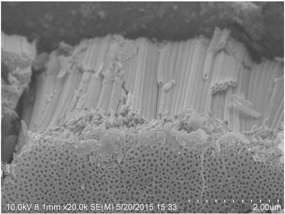
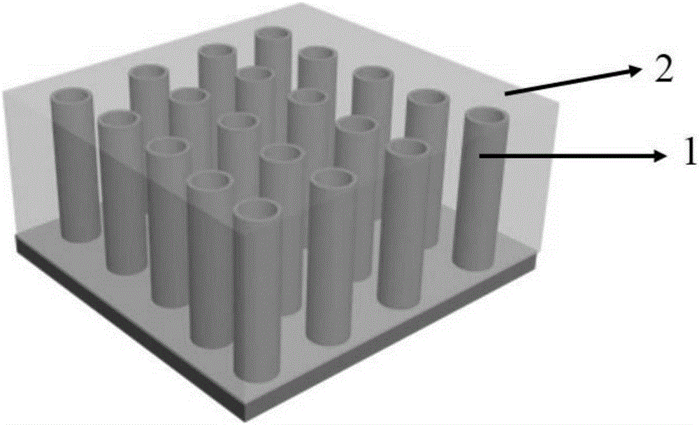
[0038] 2) The treated titanium substrate is used as the anode, and the platinum mesh is used as the cathode, containing 0.2wt% NH 4 F's ethylene glycol: water (volume ratio 50:1) solution is used as the electrolyte, and a voltage of 60V is applied to anodize the titanium substrate for 60min. After the reaction, the samples were washed with deionized water, dried and calcined in a box-type sintering furnace at 450 °C for 3 h. figure 1 It can be seen that the pore diameter of the nanotube is about 50 nm, the wall thickness is about 25 nm, and the length of t...

Embodiment 2

[0040] deposited on TiO2 The structure of dicyclohexane-perylene tetraimide (N,N-(dicyclohexyl)perylene-3,4,9,10-tetracarboxylicdiimide, CH-PTCDI) on the inner and outer surfaces of nanotubes is shown in Formula 1:

[0041]

[0042] (1)

Embodiment 3

[0044] Repeat Example 2, deposited on TiO 2 The diphenyl-perylene tetraacid diimide structure on the inner and outer surfaces of the nanotubes is shown in Formula 2:

[0045]

[0046] (2)


PUM

PropertyMeasurementUnit
Diameteraaaaaaaaaa
Tube chiefaaaaaaaaaa
Wall thicknessaaaaaaaaaa

Abstract

The invention discloses an inorganic/organic semiconductor nano-composite structure and a preparation method and an application thereof. The preparation method comprises the following steps: etching and cleaning a titanium foil serving as a substrate to obtain a titanium substrate, obtaining an inorganic semiconductor TiO<2> nanotube array on the surface of the titanium substrate by means of a positive electrode oxidation method; and depositing a layer of perylenetetracarboxylic diimide organic semiconductor film on the surface of the TiO2 nanotube array serving as a growing substrate through a physical vapor deposition method to obtain the inorganic/organic semiconductor nano-composite structure. Meanwhile, nano-composite structures with different organic film deposition amounts can be realized by changing the substrate position of the TiO<2> nanotube array. The method is simple and feasible, and an experimental basis is laid for a hierarchical assembly of inorganic and organic semiconductor materials. As proved by a result of research on the application of the obtained nano-composite structure in the field of photocatalytic hydrogen production by water decomposition of photo-electrochemical cells, the structure has efficient photocatalytic performance.

Description

technical field [0001] The invention belongs to the field of semiconductor photocatalysis, and specifically relates to an inorganic / organic semiconductor nanocomposite structure, a preparation method and its application in photoelectrochemical cell photolysis of water to produce hydrogen. Background technique [0002] With the development of society, energy shortage and environmental pollution have become the focus of people's attention. Photocatalytic technology can convert solar energy into electrical energy and chemical energy, and has broad application prospects in the fields of energy conversion and environmental governance. Among them, photoelectrochemical photolysis of water to produce hydrogen is an important aspect of solar energy utilization, which has attracted widespread attention from various countries because of its low cost and the integration of light conversion and storage. [0003] As a kind of widely used photocatalytic materials, inorganic semiconductors...

Claims


Application Information

Patent Timeline
IPC IPC(8): B81B7/04B81C1/00
Inventor 王鲁宁陈颖芝岳小琪
Owner UNIV OF SCI & TECH BEIJING
Why Eureka
Try Eureka