Hydrothermal preparation method of Sb2S3 semiconductor film with narrow band gap

A semiconductor, narrow bandgap technology, applied in the field of hydrothermal preparation of Sb2S3 semiconductor thin films, can solve the problems of large environmental pollution, unstable system, reduced solar light absorption efficiency, etc., and achieve the effect of good crystallinity and uniform and continuous thin film

Active Publication Date: 2016-07-13
BEIJING UNIV OF CHEM TECH
View PDF4 Cites 10 Cited by
  • Summary
  • Abstract
  • Description
  • Claims
  • Application Information

AI Technical Summary

Problems solved by technology

[0004] However, the reported hydrothermal preparation of Sb 2 S 3 The material has the following disadvantages: 1) The prepared Sb 2 S 3 The material is generally in the form of powder, and spin coating or spray coating is required to form a film on the substrate during the process of assembling solar cells; 2) SbCl is commonly used in solution systems 3 Provide Sb 3+ , but SbCl 3 It is easy to hydrolyze and cause the system to be unstable, so it is necessary to add some complexing agents represented by citric acid, tartaric acid and EDTA or organic solvents represented by acetone to promote SbCl 3 3) Thioacetamide and thiourea are commonly used as sulfur sources in the solution system, and these organic sulfur sources emit strong irritation during the reaction process. Ammonia, which pollutes the environment very much and causes a bad working environment
4) Sb prepared by the existing hydrothermal method 2 S 3 The bandgap value of the material is higher than the optimal bandgap value of 1.5eV for the absorbing layer of the solar cell, which reduces the absorption efficiency of sunlight
[0005] Although it has been reported that Sb 2 S 3 A chemical bath preparation method for semiconductor thin films, but has the following disadvantages: 1) The solution uses organic solvent acetone to dissolve SbCl 3 , causing great environmental pollution; 2) The prepared thin film is not uniform and continuous, which reduces the absorption efficiency of sunlight; 3) The prepared thin film has a band gap value of 2.30eV, which is much higher than the optimal band gap of the solar cell absorbing layer. The gap value is 1.5eV, which is not conducive to the absorption layer material of solar cells

Method used


Image

  • Hydrothermal preparation method of Sb2S3 semiconductor film with narrow band gap
  • Hydrothermal preparation method of Sb2S3 semiconductor film with narrow band gap
  • Hydrothermal preparation method of Sb2S3 semiconductor film with narrow band gap

Examples


Embodiment 1

[0030] 1) Weigh 0.334gKSbC in sequence 4 h 4 o 7 1 / 2H 2 O, 0.496gNa 2 S 2 o 3 ·5H 2 O (the reagents used are all analytical grade, the molar ratio is 10:20) was dissolved in 100mL aqueous solution, stirred evenly and then ultrasonicated for 5min.

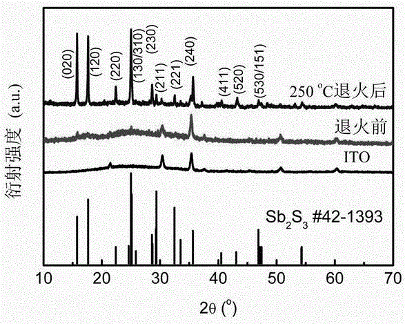
[0031] 2) Transfer the solution prepared in step 1) to the polytetrafluoroethylene liner of the hydrothermal kettle, use the pretreated ITO glass as the base, place its conductive side down, and place it obliquely in the polytetrafluoroethylene liner middle. After sealing the hydrothermal kettle and the polytetrafluoroethylene liner, the temperature of the hydrothermal kettle is controlled at 150oC, and the hydrothermal time is controlled at 8h to obtain orange-red Sb with good adhesion. 2 S 3 semiconductor film. figure 1 X-ray diffraction results show that the film has only weak Sb 2 S3 diffraction peaks, indicating its poorly crystalline structure.

[0032] 3) Under the condition of argon protection, the above Sb 2 S ...

Embodiment 2

[0034] 1) Weigh 0.334gKSbC in sequence 4 h 4 o 7 1 / 2H 2 O, 0.496gNa 2 S 2 o 3 ·5H 2 O (the reagents used are all analytical grade, the molar ratio is 10:20) was dissolved in 100mL aqueous solution, stirred evenly and then ultrasonicated for 5min.

[0035] 2) Transfer the solution prepared in step 1) to the polytetrafluoroethylene liner of the hydrothermal kettle, use the pretreated ITO glass as the substrate, place its conductive side down, and place it obliquely in the polytetrafluoroethylene liner middle. After sealing the hydrothermal kettle and the polytetrafluoroethylene liner, the temperature of the hydrothermal kettle is controlled at 150oC, and the hydrothermal time is controlled at 8h to obtain orange-red Sb with good adhesion. 2 S 3 semiconductor film.

[0036] 3) Under the condition of argon protection, the above Sb 2 S 3 The semiconductor film was placed in a tube furnace at a constant temperature of 450°C for 60 minutes, and then the film was taken out...


PUM


Abstract

The invention relates to a hydrothermal preparation method of a Sb2S3 semiconductor film with a narrow band gap. A solution contains antimony potassium tartrate and sodium hyposulfite with molar ratio of 10 to (9-80) and has a pH value from 4 to 4.5. After the solution is subjected to stirring, a Sb2S3 film with good adhesive force is directly prepared on an ITO glass substrate by means of a hydrothermal method. Then, the Sb2S3 film is maintained at certain constant temperature between 250 to 550 degrees centigrade under inert atmosphere so that the Sb2S3 semiconductor film with a narrow band gap is obtained. The novel plating solution in the method is friendly to environment. The Sb2S3 semiconductor film is directly prepared on the ITO glass substrate, has a narrow band gap, and is suitable to be used as an absorbing layer material of a thin-film solar cell.

Description

technical field [0001] The invention belongs to the field of optoelectronic materials, in particular to Sb that can be used as a narrow bandgap material for the absorbing layer of a thin film solar cell 2 S 3 Hydrothermal method for the preparation of semiconducting thin films. Background technique [0002] Sb 2 S 3 It is a typical transition metal chalcogenide, it is a typical V-VI compound, and it is a very important direct bandgap inorganic semiconductor. Its bandgap value is 1.5eV~2.2eV, at the same time, Sb 2 S 3 In the range of wavelengths less than 900nm, it exhibits a high light absorption coefficient (α≈10 5 cm -1 ). Sb 2 S 3 It has a wide response range to the sunlight spectrum and exhibits excellent photosensitivity. As a promising semiconductor material, Sb 2 S 3 Because of the above-mentioned physical properties and semiconductor properties, it has become a photoelectric material with great development potential. These excellent photoelectric proper...

Claims


Application Information

Patent Timeline
Patent Type & Authority Applications(China)
IPC IPC(8): H01L31/032H01L31/18
CPCH01L31/032H01L31/18Y02P70/50
Inventor 王峰刘萌贡永帅李志林窦美玲刘景军吉静
Owner BEIJING UNIV OF CHEM TECH
Why Eureka
Try Eureka