Vacuum film plating method

A vacuum coating and vacuum technology, applied in the field of MEMS manufacturing, can solve the problems of cumbersome process steps and achieve the effect of increasing deposition rate, simple device and small reaction space

Active Publication Date: 2017-03-15
SOUTHEAST UNIV
View PDF4 Cites 0 Cited by
  • Summary
  • Abstract
  • Description
  • Claims
  • Application Information

AI Technical Summary

Problems solved by technology

Among the above methods, in order to achieve the purpose of preparing diamond films on glass, usually only the plasma chemical vapor deposition method can be used, and engineers need to design more tedious process steps (for example, the problem of gas ratio flow rate and mold airtightness should be considered. )

Method used


Image

  • Vacuum film plating method
  • Vacuum film plating method
  • Vacuum film plating method

Examples


Embodiment 1

[0042] The vacuum coating method of the present invention comprises the following steps:

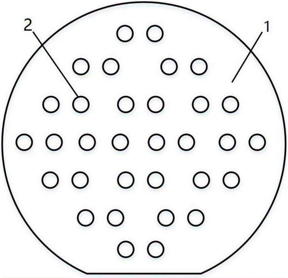
[0043] In the first step, an array of micro through-silicon holes (2) is etched on a silicon wafer (1) (for example, a 4-inch conductive wafer), and the through holes are independent and not connected to each other. The silicon wafer used may be a silicon wafer with a standard thickness, for example, a silicon wafer with a thickness of 500 microns. The diameter of the micro TSV is 1-5 mm, such as 1 mm, 1.5 mm, 1.8 mm, 2 mm, 4 mm, 5 mm. The micromachining process of the pattern structure on the silicon wafer is one of laser drilling process, wet etching process, dry inductively coupled plasma (ICP) etching process or reactive ion etching, and the pattern can be square or a circular through-hole array;

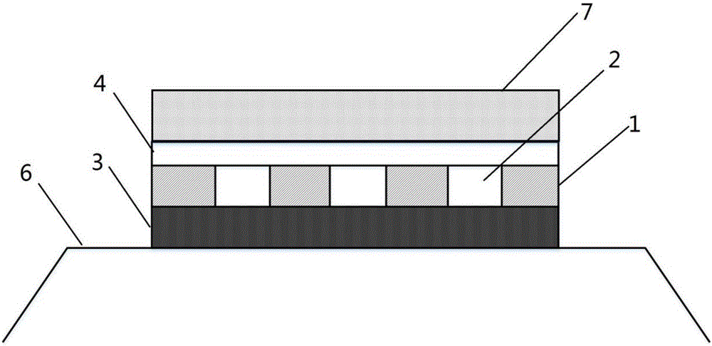
[0044] In the second step, the clean graphite disc (3) is placed on the chassis of the anodic bonding machine. mm, 4 mm, 5 mm, and then place the etched silicon wafer (1) on the graphit...

Embodiment 2

[0049] The vacuum coating method of the present invention comprises the following steps:

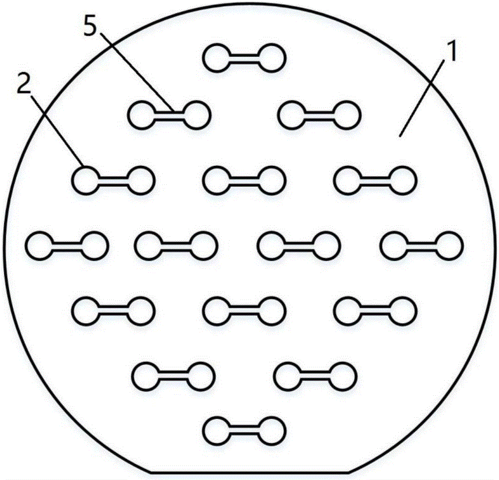
[0050] In the first step, an array of micro through-silicon holes (2) is etched on a silicon wafer (1) (for example, a 4-inch conductive wafer), and the through holes communicate with each other through channels. The silicon wafer used may be a silicon wafer with a standard thickness, for example, a silicon wafer with a thickness of 500 microns. The diameter of the micro TSV is 1-5 mm, such as 1 mm, 1.5 mm, 1.8 mm, 2 mm, 4 mm, 5 mm. The micromachining process of the pattern structure on the silicon wafer is one of laser drilling process, wet etching process, dry inductively coupled plasma (ICP) etching process or reactive ion etching, and the pattern can be square or a circular through-hole array;

[0051] The second step is to place the clean graphite disk (3) on the modified coating equipment chassis. mm, 4 mm, 5 mm, and then place the etched silicon wafer (1) on the graphite wafer ...

Embodiment 3

[0055] The vacuum coating method of the present invention comprises the following steps:

[0056] In the first step, an array of micro through holes (2) is etched on an aluminum wafer (1) (for example, a 4-inch conductive wafer), and the through holes are independent and not connected to each other. The aluminum disc used can be an aluminum disc with a standard thickness, such as an aluminum disc with a thickness of 1 mm. The diameter of the micro through hole is 1-5 mm, such as 1 mm, 1.5 mm, 1.8 mm, 2 mm, 4 mm, 5 mm. The micromachining process of the pattern structure on the silicon wafer is a laser drilling process and a wet etching process, and the pattern can be a square or circular through-hole array;

[0057] In the second step, the cleaned copper disc (3) is placed on the chassis of the anodic bonding machine. mm, 4 mm, 5 mm, and then place the etched aluminum disc (1) on the copper disc (3), and finally place the substrate disc (4). Ensure that the above-mentioned c...


PUM

PropertyMeasurementUnit
thicknessaaaaaaaaaa
thicknessaaaaaaaaaa
thicknessaaaaaaaaaa

Abstract

The invention provides a vacuum film plating method and relates to a preparation technology for a diamond-like film and a metal film. The vacuum film plating method comprises the following steps that firstly, a laser is used for cutting or sculpturing a conductive wafer (1), and through holes (2) are formed in the conductive wafer (1); secondly, a target material wafer (3), the conductive wafer (1) and a substrate wafer (4) are sequentially stacked and put in vacuum to be heated until the temperature becomes stable; and thirdly, voltage is exerted onto the target material wafer (3) and the substrate wafer (4), the target material wafer (3) is connected with the positive electrode, the substrate wafer (4) is connected with the negative electrode, and under the action of the voltage, the substrate wafer (4) is plated with a target material film (8). According to the vacuum film plating method, the area, needing to be plated with the diamond-like film or the metal film, on the substrate wafer can be precisely controlled, and the diamond-like film or the metal film with the size being a millimeter level or even a submillimeter level can be prepared.

Description

technical field [0001] The invention relates to a MEMS (micro-electro-mechanical system) manufacturing technology, in particular to a method for vacuum-coating a substrate wafer to prepare a diamond-like film or a metal film. Background technique [0002] Due to the diamond-like carbon film has a series of excellent properties such as high hardness, transparency in the infrared region, high wear resistance, low friction coefficient, high thermal conductivity, high resistivity, high chemical stability, etc., making the diamond-like carbon coating in the optical field, mechanical wear-resistant There are huge application prospects in the fields of coatings, micro-electromechanical systems and semiconductors. At present, the commonly used diamond-like film preparation processes include: ion beam enhanced deposition method, pulsed laser deposition method, cathodic arc deposition method, radio frequency plasma chemical vapor deposition method, radio frequency sputtering depositio...

Claims


Application Information

Patent Timeline
Patent Type & Authority Applications(China)
IPC IPC(8): C23C14/32C23C14/06C23C14/04
CPCC23C14/042C23C14/0605C23C14/325
Inventor 尚金堂吉宇潘智华鹿麟
Owner SOUTHEAST UNIV
Why Eureka
Try Eureka