Quantum dot light emitting diode and preparation method thereof

A quantum dot light-emitting and diode technology, which is applied in the manufacture of semiconductor/solid-state devices, electrical components, circuits, etc., can solve problems such as short life, low luminous efficiency, and unbalanced injection, and achieve good film formation and improved luminous efficiency. , Reduce the effect of injection energy barrier

Inactive Publication Date: 2017-06-06
厦门世纳芯科技有限公司
View PDF8 Cites 13 Cited by
  • Summary
  • Abstract
  • Description
  • Claims
  • Application Information

AI Technical Summary

Problems solved by technology

However, at present, the carrier injection of quantum dot light-emitting diodes is unbalanced, mainly because the rate of hole injection is much lower than the rate of electron injection, resulting in low luminous efficiency and short life.

Method used


Image

  • Quantum dot light emitting diode and preparation method thereof
  • Quantum dot light emitting diode and preparation method thereof

Examples


preparation example Construction

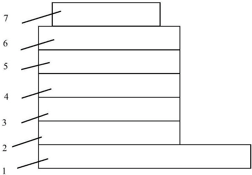
[0037] The present invention also provides a method for preparing the quantum dot light-emitting diode described in the above technical solution, comprising the following steps: sequentially depositing an anode modification layer, a hole injection layer, a hole transport layer, a quantum dot light-emitting layer, an electronic Transport layer and cathode; the anode modification layer is deposited by vacuum thermal evaporation.

[0038] In the present invention, the hole injection layer, hole transport layer, quantum dot light-emitting layer and electron transport layer are preferably deposited by spin coating.

[0039] In the present invention, the anode modification layer is vacuum thermally evaporated on the anode. In the present invention, the vacuum degree of the vapor deposition is preferably 5×10 -5 ~4×10 -4 Pa, more preferably 6~8×10 -5 Pa; In the present invention, the vapor deposition temperature is preferably 150-500°C, more preferably 200-400°C, more preferably 2...

Embodiment 1

[0051] In a vacuum of 5 x 10 -5 Pa, at a temperature of 300°C, vapor-deposit a polytetrafluoroethylene anode modification layer on an indium tin oxide anode with a thickness of 100 nm, and the thickness of the anode modification layer is 4 nm;

[0052] The following spin-coating processes were performed in an inert atmosphere of a glove box (O 2 2 O<1ppm):

[0053] Polyethylenedioxythiophene and polystyrene sulfonate were mixed at a molar ratio of 1:5, and a methanol solution was prepared at a concentration of 10mol / L, which was spin-coated at a speed of 6000r / s for 50s on the anode modification layer, and then at 150 Drying at ℃ for 30 minutes to obtain a hole injection layer with a thickness of 20 nm;

[0054] Spin-coat 10mg / mL PVK chlorobenzene solution on the surface of the hole injection layer, spin-coat at a rate of 3000r / s for 40s, put it in a vacuum drying oven at 120°C and dry for 20min to obtain a hole-transport layer with a thickness of 30nm;

[0055] Spin-coat 1...

Embodiment 2

[0061] In a vacuum of 4×10 -5 Pa, under the condition of 250°C, vapor-deposit an ethylene-tetrafluoroethylene copolymer anode modification layer on the silver nanowire anode with a thickness of 200nm, and the thickness of the anode modification layer is 6nm;

[0062] The following spin-coating processes were performed in an inert atmosphere of a glove box (O 2 2 O<1ppm):

[0063] Polyethylenedioxythiophene and polystyrene sulfonate were mixed at a molar ratio of 20:80, and an ethanol solution was prepared according to a concentration of 50mol / L, which was spin-coated at a speed of 7000r / s for 60s on the anode modification layer, and then at 150 Drying at ℃ for 25 minutes to obtain a hole injection layer with a thickness of 30 nm;

[0064] Spin-coat 8mg / mL poly-TPD chlorobenzene solution on the surface of the hole injection layer, spin-coat at a rate of 2500r / s for 40s, put it in a vacuum drying oven at 150°C for 10min, and obtain a hole transport layer with a thickness of 20...


PUM


Abstract

The invention provides a quantum dot light emitting diode comprising an anode, a hole injection layer, a hole transmission layer, a quantum dot luminescent layer, an electron transmission layer and a cathode which are arranged in turn. The quantum dot light emitting diode also comprises an anode modification layer which is arranged on the anode and the hole injection layer. The anode modification layer includes fluorine containing organic material. According to the quantum dot light emitting diode, the fluorine containing organic material acts as the anode modification layer which is arranged between the anode and the hole injection layer, and the fluorinated substituent exerts a high electron withdrawing effect by its high electronegativity so as to enhance hole injection; besides, the chemical property of the fluorine containing organic material is stable so that the luminous efficiency of the quantum dot light emitting diode can be stably enhanced and the service life can be prolonged.

Description

technical field [0001] The invention relates to the technical field of quantum dot light emitting diodes, in particular to a quantum dot light emitting diode and a preparation method thereof. Background technique [0002] Quantum dots are quasi-zero-dimensional nanomaterials composed of a small number of atoms. Quantum dots belong to inorganic semiconductor materials, which have more stable photochemical stability than organic materials, and can realize the regulation of fluorescence wavelength and emission spectrum by adjusting the size of quantum dots, and have excellent fluorescence quantum yield. Due to their excellent properties, quantum dots have attracted widespread attention and are widely used in the field of display technology. [0003] Quantum dot light-emitting diode (QLED) is a quantum dot organic light-emitting device that uses quantum dots as the light-emitting layer and can generate and emit light of any visible wavelength. Quantum dot light-emitting diodes...

Claims


Application Information

Patent Timeline
Patent Type & Authority Applications(China)
IPC IPC(8): H01L51/54H01L51/50H01L51/56
CPCH10K85/141H10K85/151H10K50/17H10K71/00
Inventor 顾小兵魏居富蒋杰张青松
Owner 厦门世纳芯科技有限公司
Why Eureka
Try Eureka