Double-purpose mass spectrum detection kit

A dual-purpose, time-of-flight mass spectrometry technology, applied in the field of mass spectrometry detection, can solve problems such as low signal-to-noise ratio, high baseline, and poor crystal morphology

Active Publication Date: 2017-09-22
BIOYONG TECH
View PDF6 Cites 8 Cited by
  • Summary
  • Abstract
  • Description
  • Claims
  • Application Information

AI Technical Summary

Problems solved by technology

[0017] Although MALDI-TOF time-of-flight mass spectrometry can be used to detect proteins or nucleic acid molecules, from the application point of view, the traditional MALDI chip has a single application field, such as the DE1580TA steel target plate produced by SHIMADZU, which is only used for the identification of protein microorganisms and is suitable for The MALDI-TOF AXIMA of SHIMADZU; the L24 SpectroCHIP chip produced by AGENA is only used for genetic testing and is suitable for AGENA's MALDI-TOF MASSARRY. At present, there is no chip that can cover both genomics testing and proteomics identification.
[0018] From the perspective of the material and surface characteristics of the mass spectrometer chip, the traditional

Method used


Image

  • Double-purpose mass spectrum detection kit
  • Double-purpose mass spectrum detection kit
  • Double-purpose mass spectrum detection kit

Examples


Embodiment 1

[0096] Embodiment 1, microarray chip surface hydrophilic treatment

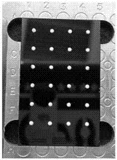
[0097] The main feature of the chip is tough texture and good flatness; diamond, single crystal silicon, quartz crystal, etc.; divided into a sheet structure suitable for the size of the surface unit of the chip adapter, the thickness of the chip is 0.5-1.8mm, in order to ensure the accuracy of quality inspection, the surface of the chip The flatness is less than 10μm. For example, a single crystal silicon wafer is selected as the substrate of the microarray chip, and silicon dioxide oxide films, zinc oxide films, and aluminum oxide films can be fired and grown on the surface of the silicon wafer structure, with a thickness of 150-800nm, preferably 500nm. Water-based, using thermal oxidation process.

[0098] Such as image 3 As shown, the steps of using a thermal oxidation device to burn and grow a silicon dioxide oxide film are as follows:

[0099] ① Place the silicon wafer in a reaction tube made of qua...

Embodiment 2

[0107] Embodiment 2, microarray chip surface hydrophobic treatment

[0108] 1. Sealing treatment of hydrophilic spotting hole area

[0109] Clean residual organic matter on the surface of the chip: first pass the oxygen flow rate of 60-140ml / min, the power of 100-300W, and the treatment time of 1-10min; Thoroughly cleansed and hydroxylated.

[0110] Photoresist technology to seal the sample hole area: Spin the photoresist on the treated substrate by spin coating, the spin coating speed is 1000 ~ 8000rpm, and then place it under the photolithography mask plate, in the 390nm ultraviolet After being exposed to light for 20s~5min, it is eluted with the corresponding developer, so as to construct the spotting hole area with an ordered structure. The photoresist uses acid-resistant polymethyl methacrylate (PMMA) and / or polystyrene.

[0111] 2. Hydrophobic treatment of the outer area of ​​the microarray chip hole

[0112] The process of surface treatment of metal or non-metal mat...

Embodiment 3

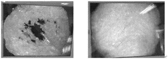
[0137] Example 3: Crystallization comparison between microarray dual-purpose chip and traditional chip

[0138] Select the same protein or nucleic acid sample, and take an appropriate amount of the corresponding matrix solution and drop them on the dual-purpose chip and the traditional chip respectively. After the matrix is ​​naturally dried, observe the crystal form under the microscope.

[0139] Such as Figure 5 As shown, the crystal form of the traditional biological detection chip (left picture) is irregular, the thickness is uneven, and it is in the shape of a coffee ring, with a hollow center and thick surroundings. However, the microarray chip provided by the present invention has regular crystal morphology (right picture), uniform thickness, and fine crystal growth.


PUM

PropertyMeasurementUnit
Thicknessaaaaaaaaaa
Apertureaaaaaaaaaa
Thicknessaaaaaaaaaa

Abstract

The invention provides a general chip for carrying out mass spectrum detection on proteins and nucleic acid during flight time. The chip comprises (1) a chip main body and (2) a chip adapter, wherein the surface of the main body is provided with a hydrophilic sampling hole and a hydrophobic hole outer area which are arranged in a micro-column form; the chip adapter is formed by a metal bottom plate, wherein a plurality of chip slots matched with the chip main body are distributed on a surface of the adapter, and the chip main body is selected from chips of single-sided polished diamonds, monocrystalline silicon and quartz crystals which are strong in texture and good in flatness; the hydrophilic sampling hole covers a hydrophilic film with the thickness of 150 to 800nm, the hydrophobic hole outer area covers a hydrophobic film with the thickness of 150nm to 2mu m, and a surface water droplet contact angle is more than 120 degrees; a sampling hole is pre-processed by using a coverage matrix solution in advance, and the matrix solution is selected from the matrix solution for protein mass spectrum, or the matrix solution is selected from the matrix solution for nucleic acid mass spectrum.

Description

technical field [0001] The invention relates to a dual-purpose chip for detecting protein and nucleic acid by time-of-flight mass spectrometry, which can detect protein and nucleic acid molecules by mass spectrometry, and belongs to the field of mass spectrometry detection. Background technique [0002] Proteomics is a new science in the era of functional genomics, which studies the composition, activity rules and protein-protein interactions of intracellular proteins from an overall level. Including the identification of protein expression, modified form, structure, function and interaction. According to the research purpose, proteomics can be divided into expression proteomics, structural proteomics and functional proteomics. Expression proteomics is used to quantitatively study the expression of protein samples in cells. The purpose of proteomics is to map out the structure of protein complexes or proteins present in a special organelle, called structural proteomics, wh...

Claims


Application Information

Patent Timeline
IPC IPC(8): G01N27/64G01N1/28
CPCG01N1/28G01N27/64
Inventor 马庆伟梁飞党文娟
Owner BIOYONG TECH
Why Eureka
Try Eureka