A kind of preparation method of large-scale gallium nitride semiconductor chip for LED

A gallium nitride and semiconductor technology, applied in semiconductor devices, electrical components, circuits, etc., can solve problems such as high density, mismatched lattice, small size, etc., and achieve simple preparation process, easy storage and transportation, and wide sources Effect
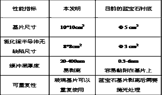
Active Publication Date: 2019-06-14
启东盛丽光电科技有限公司
View PDF3 Cites 0 Cited by
  • Summary
  • Abstract
  • Description
  • Claims
  • Application Information

AI Technical Summary

Problems solved by technology

However, this process has a small size of hexagonal boron nitride, which is not conducive to the use of large-scale substrates
[0008] In summary, the existing GaN substrates mostly use sapphire, silicon carbide and silicon, but the degree of lattice mismatch leads to the formation of defects that limit light emission in the GaN film.
The use of nanomaterials to improve GaN substrate technology has appeared, but this technology still has defects with high defect density and small size.

Method used


Image

  • A kind of preparation method of large-scale gallium nitride semiconductor chip for LED

Examples


Embodiment 1

[0034] (1) Add ethyl orthosilicate to methanol solvent, control the temperature at 25°C, and stir at 300 rpm, then add deionized water and 7% hydrochloric acid in sequence, and adjust the pH value to between 3-4 Between, obtain silica airgel precursor liquid, the ratio of described ethyl orthosilicate, methyl alcohol, deionized water, 7% hydrochloric acid is 1:5:2:1 in molar ratio;

[0035] (2) After the silica airgel precursor solution was left to stand at a temperature of 30°C for 0.1 hour, the temperature was adjusted to 60°C, and the drying control additive formamide was added under the condition of a stirring speed of 200 rpm Stir for 10-20 minutes, the molar ratio of tetraethyl orthosilicate and formamide is 1:0.25;

[0036] (3) Add alumina with a particle size of 100nm to the silica airgel obtained in step (2), stir for 5 minutes at a stirring speed of 300 rpm, then add ammonia water, and stir for 5 minutes to obtain Aluminum-silica airgel composite sol;

[0037] (4) Sp...

Embodiment 2

[0041] (1) Add methyl orthosilicate to ethanol, set the temperature of ethanol at 35°C, and stir at 350 rpm, then add distilled water and 10% hydrochloric acid in turn to adjust the pH value to between 3-4 Between, obtain silica airgel precursor solution, the ratio of described methyl orthosilicate, ethanol, distilled water, 10% hydrochloric acid is 1:6:4:2 in molar ratio;

[0042] (2) After the silica airgel precursor solution was allowed to stand at 40°C for 1 hour, the temperature was adjusted to 65°C, and the drying control additive acetamide was added at a stirring speed of 350 rpm Stir for 10-20 minutes, the molar ratio of the silicon alkoxide and acetamide is 1:0.35;

[0043] (3) Add alumina with a particle size of 300nm to the silica airgel obtained in step (2), stir for 20 minutes at a stirring speed of 350 rpm, then add sodium hydroxide, and stir for 15 minutes. Obtain alumina-silica airgel composite sol;

[0044] (4) Spin the alumina-silica airgel composite sol on...

Embodiment 3

[0048] (1) Add propyl silicate to isopropanol, set the temperature of isopropanol solvent to 35°C, and stir at 500 rpm, then add deionized water and 15% hydrochloric acid in turn to adjust its pH Value is between 3-4, obtains silica airgel precursor liquid, and the ratio of described propyl silicate, isopropanol, deionized water, 15% hydrochloric acid is 1:5:4:3 in molar ratio ;

[0049] (2) After the silica airgel precursor solution was left to stand at a temperature of 50°C for 5 hours, the temperature was adjusted to 70°C, and the drying control additive acetamide was added at a stirring speed of 300 rpm Stir for 15 minutes, the molar ratio of propyl silicate and N,N-dimethylformamide is 1:0.3;

[0050] (3) Add alumina with a particle size of 400nm to the silica airgel obtained in step (2), stir for 25 minutes at a stirring speed of 400 rpm, then add ammonium fluoride, and stir for 25 minutes , to obtain alumina-silica airgel composite sol;

[0051] (4) Spin the alumina-...


PUM

PropertyMeasurementUnit
particle diameteraaaaaaaaaa

Abstract

The invention proposes a fabrication method of a large-size GaN semiconductor sheet for an LED. The fabrication method comprises the steps of fabricating a large-area GaN substrate by taking silicon dioxide aerogel and aluminum oxide as raw materials; mixing the silicon dioxide aerogel and the aluminum oxide to obtain aluminum oxide-silicon dioxide aerogel composite sol, performing coating process, coating the aluminum oxide-silicon dioxide aerogel composite sol on a surface of ordinary glass, forming a composite substrate material by a sintering process, and performing deposition to grow the large-size GaN semiconductor. Due to the scalability, the high-temperature resistance and the strippability of the silicon dioxide aerogel, the obtained GaN is large in size and complete in lattices and has no defect; and moreover, the substrate fabricated according to the method can be repeatedly used, is low in cost and simple in process, and is suitable for industrial production on a large scale.

Description

technical field [0001] The invention relates to the field of preparation of luminescent materials, in particular to a method for preparing large-sized gallium nitride semiconductor chips for LEDs. Background technique [0002] A light-emitting diode is a type of semiconductor diode that can convert electrical energy into light energy; it is often abbreviated as LED. Like ordinary diodes, light-emitting diodes are composed of a PN junction and also have unidirectional conductivity. When a forward voltage is applied to the light-emitting diode, the holes injected from the P region to the N region and the electrons injected from the N region to the P region are respectively connected to the electrons in the N region and the vacancies in the P region within a few microns near the PN junction. Hole recombination, resulting in spontaneous emission of fluorescence. The energy states of electrons and holes are different in different semiconductor materials. The amount of energy r...

Claims


Application Information

Patent Timeline
Patent Type & Authority Patents(China)
IPC IPC(8): H01L33/32H01L33/00H01L33/20
CPCH01L33/0075H01L33/20H01L33/32
Inventor 陈庆曾军堂陈兵
Owner 启东盛丽光电科技有限公司
Why Eureka
Try Eureka