
Light emitting diode apparatus and display apparatus

A technology of light-emitting diodes and light-emitting layers, applied in electrical components, circuits, organic semiconductor devices, etc., can solve problems such as low internal quantum efficiency, low conductivity, and difficulty in injecting carriers into quantum dots

Active Publication Date: 2018-08-10
SUZHOU XINGSHUO NANOTECH CO LTD
View PDF4 Cites 11 Cited by
  • Summary
  • Abstract
  • Description
  • Claims
  • Application Information

AI Technical Summary

Problems solved by technology

The main disadvantage of the second type of QLED is its low internal quantum efficiency, which is derived from the existence of energy level barriers in quantum dots, especially when they are coated with a layer of organic ligands, due to the low conductivity of semiconductor nanocrystals. , making it more difficult for carriers to be injected into the quantum dots, thus exacerbating the problem of low quantum efficiency

Method used


Image

  • Light emitting diode apparatus and display apparatus
  • Light emitting diode apparatus and display apparatus
  • Light emitting diode apparatus and display apparatus

Examples


Embodiment 1

[0128] Synthesis of P8 molecule:

[0129] Under an argon atmosphere, 3.29g (6mmol) of 2,7-dibromo-9,9-dioctylfluorene was dissolved in 80ml of anhydrous tetrahydrofuran, and the temperature was lowered to -78°C (dry ice-acetone bath). 5.1 ml of n-butyl lithium (2.5M in hexane; 12.75 mmol) was slowly added dropwise to give a thick bright yellow solution. Stirring was continued at -70°C for 20 min, then the temperature of the reaction mixture was raised to 0°C. Then the temperature was raised to normal temperature, and 2.8 g (12.75 mmol) of diphenylphosphine chloride were added. The reaction was stirred at -70°C for an additional 3 hours before quenching with 2 ml of degassed methanol. The volatiles were removed under reduced pressure to leave an oily liquid. The crude material was purified by column chromatography on silica (Rf=0.29) with chloroform / n-hexane (2:8) as mobile phase, finally yielding 3.50 g (77%) of chemically pure P8.

Embodiment 2

[0131] Synthesis of PO8 molecules:

[0132] Mix 3.03 g (4 mmol) of P8, 50 ml of dichloromethane and 10 ml of 30% hydrogen peroxide solution, and mix and stir overnight at room temperature. The organic layer was separated and washed successively with water and brine. The product was evaporated to dryness to give a white solid, which was further purified by recrystallization from toluene / n-hexane to give 2.7 g (85%) of chemically pure PO8.

Embodiment 3

[0134] Pre-treatment and cleaning of pre-patterned ITO flakes:

[0135] Set 12 pre-patterned ITO chips covered with polymer on the glass substrate, and immerse in 5% sodium hydroxide aqueous solution at 80° C. for 5 min. Repeat the above steps, and then wash the chip with nanopure water and 20% ethanolamine aqueous solution, and sonicate for 15 minutes, then wash and dry with sufficient nanopure water. Finally, load the ITO chip into the plasma cleaning chamber to clean the surface of the ITO-coated device.


PUM


Abstract

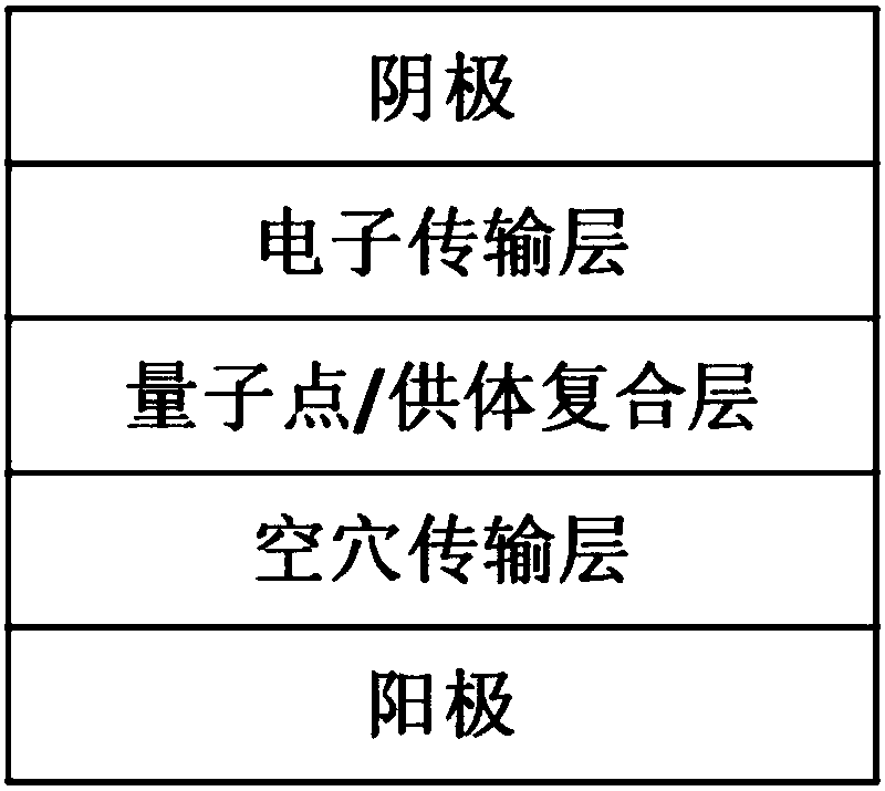
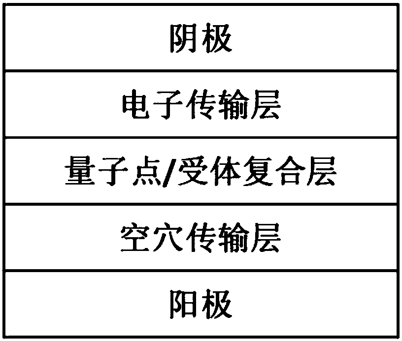
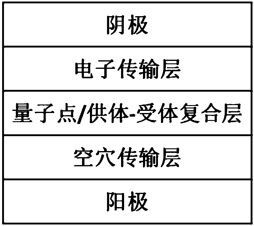
The invention provides a light emitting diode apparatus. The light emitting diode apparatus comprises a substrate, a positive electrode, a hole transport layer, a light emitting layer, an electron transport layer and a negative electrode; the light emitting diode apparatus is characterized in that the light emitting layer is formed by quantum dots and energy transfer molecules in a combination manner; and the energy transfer molecules and the quantum dots are crosslinked through click chemistry. The energy transfer molecules, used as the dispersion medium of the quantum dots, have high electron / hole carrier injection capability, so that exciton generation in the energy transfer molecules can be promoted, and effective energy transfer from the energy transfer molecules to fluorescent quantum dots can be realized; and at a certain voltage, the apparatus can give out light within a wavelength range of 380-900nm, and the maximum emitting peak value is from ultraviolet light to deep infrared light. The invention also discloses a preparation method of the light emitting diode apparatus and electronic display apparatus.

Description

[0001] divisional application [0002] This application is a divisional application of the Chinese patent application "201610704608.1" filed on August 23, 2016, entitled "Light-emitting diode device including quantum dots and energy transfer molecules, its preparation method, and display device". technical field [0003] The present application belongs to the display field, and in particular relates to a light emitting diode device and a display device. Background technique [0004] Quantum dots are nanometer-sized semiconductor nanocrystals with controllable surface chemical states and size-dependent optical properties. Quantum dots can be photoluminescent and electroluminescent. In display device applications, quantum dots are not inferior to organic light-emitting diodes (OLEDs), and have the following advantages: 1) lifetime, quantum dots are composed of inorganic cores, and have a potentially long life; 2) color purity, quantum dots produce There are many kinds of co...

Claims


Application Information

Patent Timeline
Patent Type & Authority Applications(China)
IPC IPC(8): H01L51/54H01L51/50H01L51/56
CPCH10K85/111H10K85/649H10K50/115H10K2102/00H10K71/00H10K50/00H10K50/121
Inventor 王允军
Owner SUZHOU XINGSHUO NANOTECH CO LTD
Learn More