A kind of all-inorganic perovskite photodetector and its preparation method

A photodetector, inorganic calcium technology, used in circuits, electrical components, semiconductor devices, etc., can solve the problems of inability to obtain high crystalline quality films, thick charge transport layer film thickness, insufficient detection sensitivity limit, etc. Photoelectric responsivity, beneficial to absorption, and the effect of reducing the dark current of the device

Active Publication Date: 2021-06-11
JINAN UNIVERSITY
View PDF11 Cites 0 Cited by
  • Summary
  • Abstract
  • Description
  • Claims
  • Application Information

AI Technical Summary

Problems solved by technology

On the one hand, this is due to the limitations of the preparation method of inorganic perovskite films, which cannot obtain high-quality crystalline films, and the thickness of the charge transport layer film is too thick and difficult to control; on the other hand, it is due to the device structure design, which leads to interface defects. State introduction, photogenerated charge recombination increases
The above reasons lead to the large dark current of most of the reported devices, insufficient detection sensitivity limit and low responsivity

Method used


Image

  • A kind of all-inorganic perovskite photodetector and its preparation method
  • A kind of all-inorganic perovskite photodetector and its preparation method
  • A kind of all-inorganic perovskite photodetector and its preparation method

Examples


Embodiment 1

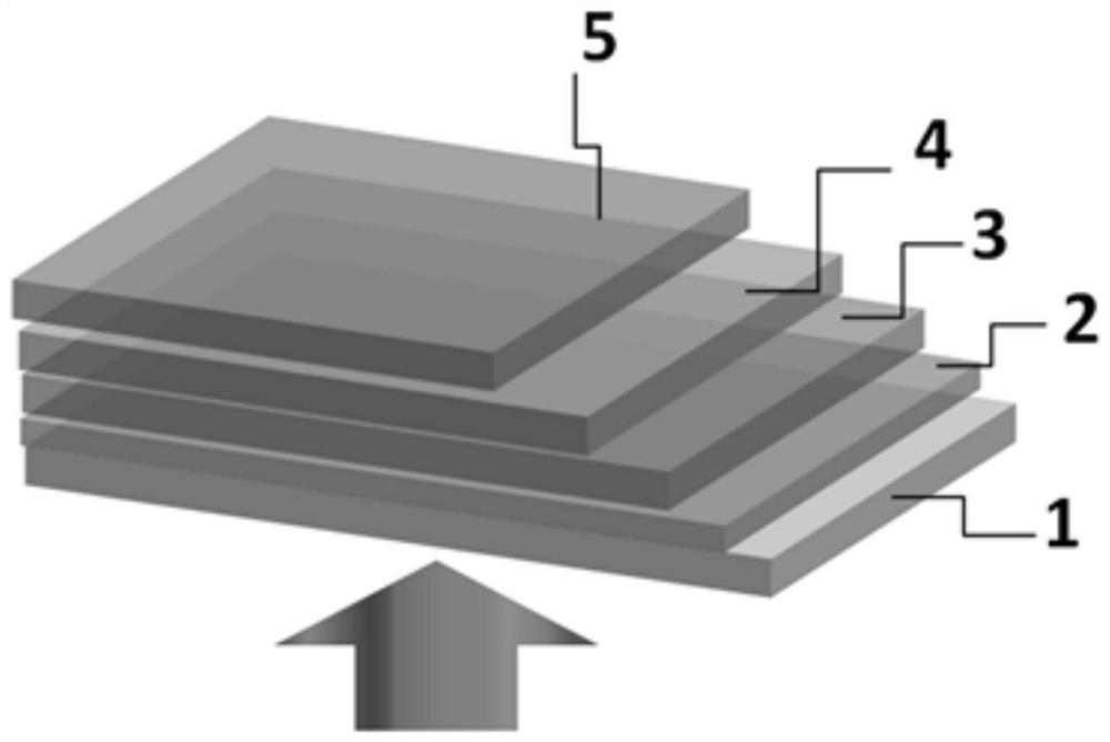
[0049] (1) The commercial FTO was partially etched by the mixed reaction of dilute hydrochloric acid (HCl) and zinc powder (Zn), and then the substrate was ultrasonically cleaned in deionized water, acetone and isopropanol for 15 minutes each; The substrate was blown dry with nitrogen, and treated with ultraviolet ozone for 30 minutes.

[0050] (2) Deposit a layer of aluminum oxide film with a thickness of 1.5nm on the substrate treated by (1) by ALD technology (model: BENEQ, TFS200), the precursor source is trimethylaluminum (TMA), and the deposition conditions are: The chamber temperature was 85° C., the chamber pressure was 9 Pa, and the growth cycle was 16 times.

[0051] (3) Dissolve 0.33mol cesium bromide and 0.33mol lead bromide in 1mL dimethyl sulfoxide solution, heat and stir at 70°C for 12h to obtain CsPbBr 3 Precursor solution: Spin-coat the precursor solution on the aluminum oxide film, the spin-coating conditions are: spin-coating at 500rpm for 6 seconds, and spi...

Embodiment 2

[0056] 1. With reference to Example 1, only the thickness of the aluminum oxide thin film layer in step (2) is made into 1nm by ALD technology, wherein the growth cycle is 11 times, and other process parameters are the same as in Example 1 to obtain an all-inorganic perovskite photoelectric detector. The device has low dark current and high stability.

[0057] 2. With reference to Example 1, only the thickness of the aluminum oxide film layer in step (2) is made into 3nm by ALD technology, wherein the growth cycle is 32 times, and other process parameters are the same as in Example 1 to obtain an all-inorganic perovskite photoelectric detector. The device has low dark current and high stability.

[0058] 3. With reference to Example 1, only the thickness of the titanium oxide film layer in step (4) is made into 5nm by ALD technology, wherein the growth cycle is 86 times, and other process parameters are the same as in Example 1 to obtain an all-inorganic perovskite photoelec...

Embodiment 3

[0061] With reference to Example 1, only the commercial FTO in step (1) is changed into PET / ITO, and other process parameter conditions are the same as in Example 1 to obtain an all-inorganic perovskite photodetector, and its current-time curve is as follows Figure 9 shown.


PUM

PropertyMeasurementUnit
thicknessaaaaaaaaaa
thicknessaaaaaaaaaa
thicknessaaaaaaaaaa

Abstract

The invention discloses an all-inorganic perovskite photodetector and a preparation method thereof. The photodetector with an inverted structure includes a transparent conductive positive electrode, an ultra-thin aluminum oxide layer, an all-inorganic perovskite light absorption layer, an electron transport layer, and a metal negative electrode. The preparation method adopts ALD to deposit ultra-thin aluminum oxide film and titanium oxide film, and the obtained device has low dark current and high stability, and the device still exhibits good photoelectric performance after being exposed to air for more than 100 days. An ultra-thin titanium oxide film is introduced at the interface between the perovskite and the metal electrode to achieve interface energy band matching and improve the response speed and sensitivity of the device. The preparation method of the invention is suitable for making flexible detectors, and provides an effective, feasible and low-cost solution for realizing the industrialization of inorganic perovskite photodetectors and flexible devices thereof.

Description

technical field [0001] The invention belongs to the technical field of novel all-inorganic semiconductor photoelectric detection preparation, and in particular relates to a high-stability, low-dark-current all-inorganic perovskite photodetector and a preparation method thereof. Background technique [0002] Organic / inorganic hybrid metal halide perovskites (the general chemical formula is ABX 3 ) has excellent photoelectric properties such as long carrier diffusion distance, high carrier mobility, large light absorption coefficient, and long exciton diffusion distance, and is widely used in optoelectronic applications; such as solar cells, photodetectors, light emitting Diode, quantum dot display and other fields. In recent years, thanks to the suitable band gap and high absorption coefficient of perovskite cells, organic / inorganic hybrid perovskite materials are considered to be the most suitable optoelectronic materials for building high-performance detectors. In 2014, t...

Claims


Application Information

Patent Timeline
Patent Type & Authority Patents(China)
IPC IPC(8): H01L31/18H01L31/0216
CPCY02P70/50
Inventor 赵传熙麦文杰岑国标
Owner JINAN UNIVERSITY
Why Eureka
Try Eureka