Perovskite photoelectric detector based on composite electron transport layer and preparation method of perovskite photoelectric detector

An electron transport layer, photodetector technology, applied in the direction of electric solid device, semiconductor/solid state device manufacturing, circuit, etc., can solve the problems of short life, high device dark current, poor stability of inorganic photodetector devices, etc., to achieve good barrier Effects of water oxygen, dark current reduction, and carrier transport capability improvement

Active Publication Date: 2019-06-21
UNIV OF ELECTRONICS SCI & TECH OF CHINA
View PDF4 Cites 10 Cited by
  • Summary
  • Abstract
  • Description
  • Claims
  • Application Information

AI Technical Summary

Problems solved by technology

[0005] The invention provides a perovskite photodetector based on a composite electron transport layer and a preparation method thereof, which solves the problems of poor stability, short service life and high dark current of an inorganic photodetector

Method used


Image

  • Perovskite photoelectric detector based on composite electron transport layer and preparation method of perovskite photoelectric detector
  • Perovskite photoelectric detector based on composite electron transport layer and preparation method of perovskite photoelectric detector
  • Perovskite photoelectric detector based on composite electron transport layer and preparation method of perovskite photoelectric detector

Examples


Embodiment 1

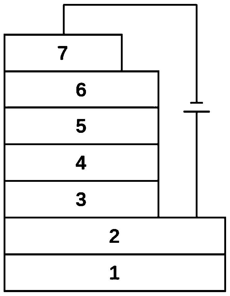
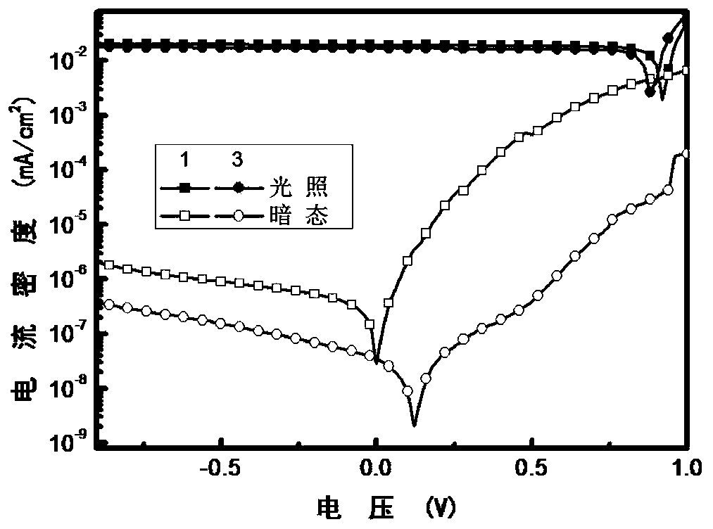
[0053] The substrate composed of the substrate and the transparent conductive anode ITO is cleaned, and dried with nitrogen after cleaning; the surface of the transparent conductive anode ITO is spin-coated with PEDOT:PSS (water dispersion, containing 1 to 3 wt% of PEDOT:PSS, spin-coating time 60s, thickness 15nm) prepare hole transport layer, and the formed film is carried out thermal annealing (annealing temperature 150 ℃, annealing time 15min); Spin-coat MAPbl on hole transport layer 3 (using DMF as a solvent to form a mixed solution with a solute concentration of 800mg / mL, the spin-coating speed is 4000rpm, the spin-coating time is 30s, and the thickness is 500nm) to prepare the perovskite photoactive layer. The carbon layer was quickly added dropwise with chlorobenzene solution to inhibit the disordered crystallization of perovskite, and then annealed at 120 °C for 20 min; the surface of perovskite photoactive layer was spin-coated with PCBM solution (aqueous dispersion so...

Embodiment 2

[0055] The substrate composed of the substrate and the transparent conductive anode ITO is cleaned, and dried with nitrogen gas after cleaning; the surface of the transparent conductive anode ITO is spin-coated with PEDOT:PSS (water dispersion, containing 1 to 3 wt% of PEDOT:PSS, spin-coating time 60s, thickness 15nm) prepare hole transport layer, and the formed film is carried out thermal annealing (annealing temperature 150 ℃, annealing time 15min); Spin-coat MAPbl on hole transport layer 3 (using DMF as a solvent to form a mixed solution with a solute concentration of 800mg / mL, the spin-coating speed is 4000rpm, the spin-coating time is 30s, and the thickness is 500nm) to prepare the perovskite photoactive layer. The carbon layer was quickly dripped with chlorobenzene solution to inhibit the disordered crystallization of perovskite, and then annealed at 120 ° C for 20 min; the surface of the perovskite photoactive layer was spin-coated with a PCBM solution doped with 2% gela...

Embodiment 3

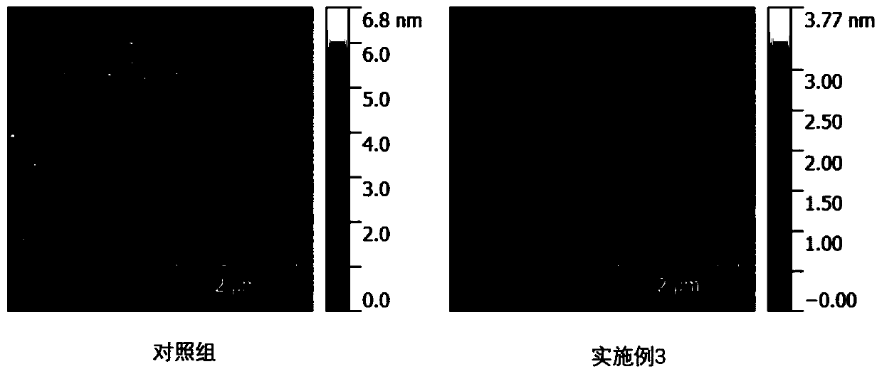
[0057] The substrate composed of the substrate and the transparent conductive anode ITO is cleaned, and dried with nitrogen after cleaning; the surface of the transparent conductive anode ITO is spin-coated with PEDOT:PSS (water dispersion, containing 1 to 3 wt% of PEDOT:PSS, spin-coating time 60s, thickness 15nm) prepare hole transport layer, and the formed film is carried out thermal annealing (annealing temperature 150 ℃, annealing time 15min); Spin-coat MAPbl on hole transport layer 3 (using DMF as a solvent to form a mixed solution with a solute concentration of 800mg / mL, the spin-coating speed is 4000rpm, the spin-coating time is 30s, and the thickness is 500nm) to prepare the perovskite photoactive layer. The carbon layer was rapidly dripped with chlorobenzene solution to inhibit the disordered crystallization of perovskite, and then annealed at 120 ° C for 20 min; the surface of the perovskite photoactive layer was spin-coated with a PCBM solution doped with 3% gelatin ...


PUM


Abstract

The invention relates to a perovskite photoelectric detector based on a composite electron transport layer. The perovskite photoelectric detector structurally comprises a substrate, a conductive anode, a hole transport layer, a perovskite photoactive layer, a composite electron transport layer, a hole barrier layer and a metal cathode from bottom to top sequentially, wherein the composite electrontransport layer is formed by a mixture of PCBM and gelatin; and the composite electron transport layer comprises 0.1%-6% by mass of gelatin and the balance PCBM. With the adoption of the composite electron transport layer doped with a bioactive material, namely, gelatin, the surface topography of an original PCBM electron transport layer is improved, so that an original mesoporous interface becomes uniform and compact, the device has better water oxygen resistance and anti-ultraviolet capability, the stability of the perovskite photoelectric detector is improved, and the working life is prolonged; besides, the carrier transport capability of the electron transport layer is improved, leakage current in work of devices is reduced, dark current is substantially reduced, and finally, the detection performance of the perovskite photoelectric detector is improved.

Description

technical field [0001] The invention relates to the technical field of photodetection devices, in particular to a perovskite photodetector based on a composite electron transport layer and a preparation method thereof. Background technique [0002] Light is a form of electromagnetic radiation. Optical radiation has a huge impact on human activities. Perceiving and measuring optical signals is of great significance to our daily life and social production. Therefore, people have begun to conduct photoelectric detection that can accurately measure optical radiation signals. device research. A photodetector is a photoelectric conversion device, which can use the photoelectric effect to convert the optical signal of the electromagnetic radiation carrying energy into a precise electrical signal, usually a photocurrent or photovoltage. High-performance photodetection is of great significance in both scientific and industrial circles. Broad-spectrum photodetectors have applications...

Claims


Application Information

Patent Timeline
Patent Type & Authority Applications(China)
IPC IPC(8): H01L51/46H01L51/42H01L51/44H01L51/48B82Y40/00
CPCY02E10/549
Inventor 杨根杰王子君高瞻于军胜
Owner UNIV OF ELECTRONICS SCI & TECH OF CHINA
Why Eureka
Try Eureka