
A laminated structure for enhancing the fluorescence luminous intensity of luminescent film and its preparation method

A technology of stacked structure and luminous intensity, applied in the field of luminescent materials, can solve the problems of high electron drift saturation speed, insignificant luminous enhancement effect, and low luminous intensity of materials, and achieve enhanced luminous intensity, low preparation cost, and time-consuming process short effect

Active Publication Date: 2021-01-01
BEIJING UNIV OF TECH
View PDF3 Cites 0 Cited by
  • Summary
  • Abstract
  • Description
  • Claims
  • Application Information

AI Technical Summary

Problems solved by technology

[0002] The third-generation semiconductor materials are widely used in blue, green, and purple light-emitting diodes and semiconductor lasers because of their large band gap, high electron drift saturation speed, and small dielectric constant; at the same time, semiconductor lighting has also become However, due to the low luminous intensity of some materials, it has become an obstacle to its practical application. Improving the luminous efficiency of materials is particularly important for large-scale applications in related fields.
Metal surface plasmons mainly enhance the local field through resonant coupling with semiconductor materials, thereby improving the luminous efficiency of the material, but for high-quality semiconductor material single crystals or thin films with high internal quantum efficiency and low defect luminescence , the luminous enhancement effect is not obvious

Method used


Image

  • A laminated structure for enhancing the fluorescence luminous intensity of luminescent film and its preparation method
  • A laminated structure for enhancing the fluorescence luminous intensity of luminescent film and its preparation method
  • A laminated structure for enhancing the fluorescence luminous intensity of luminescent film and its preparation method

Examples


preparation example Construction

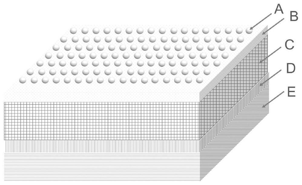
[0056] An embodiment of the present invention provides a laminated structure that enhances the fluorescence luminous intensity of a luminescent film, specifically as figure 1 As shown, it includes a single-layer dielectric microsphere array, a second metal nanoparticle layer, a luminescent film, a first metal nanoparticle layer and a substrate that are sequentially stacked and connected; the preparation method includes:

[0057] (1) cleaning and drying the substrate;

[0058] (2) Using a vacuum ion sputtering apparatus, selecting a suitable metal target, adjusting the pressure of the sample chamber and the sputtering current, and sputtering the first metal nanoparticle layer on the surface of the substrate;

[0059] (3) Prepare a luminescent film on the upper surface of the first metal nanoparticle layer by molecular beam epitaxy, magnetron sputtering or pulse laser deposition. For example, the specific steps for preparing a luminescent film zinc oxide luminescent film by puls...

Embodiment 1

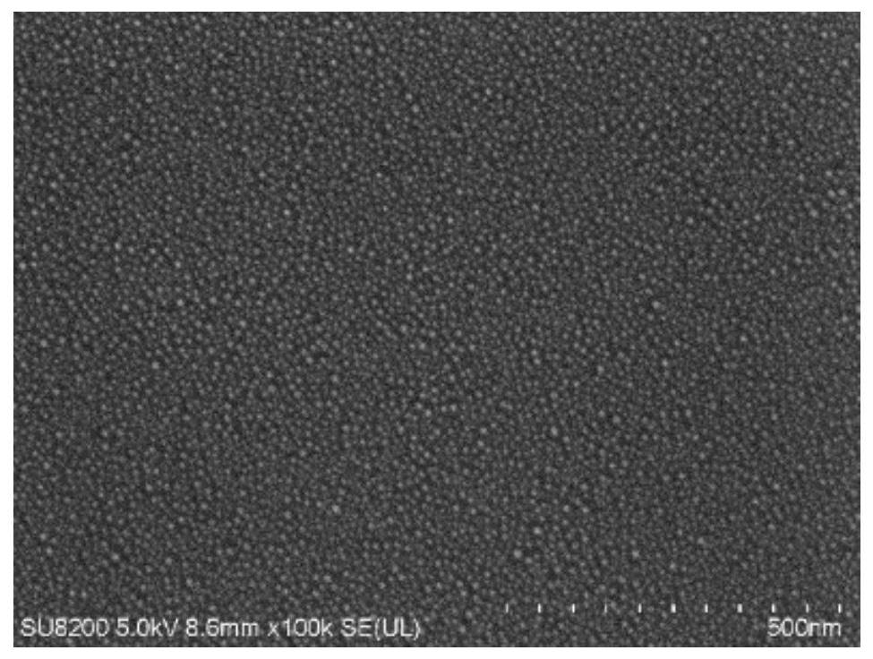
[0063] Clean the alumina single crystal substrate, and after it is naturally dried at room temperature, put it on the sample stage of the ion sputtering instrument. The sputtering time is set to 30s, so that the gold nanoparticles are uniformly deposited on the alumina substrate, and the particle size of the nanoparticles is about 16nm. The scanning electron microscope micrograph of the prepared gold nanoparticles is as follows figure 2 shown.

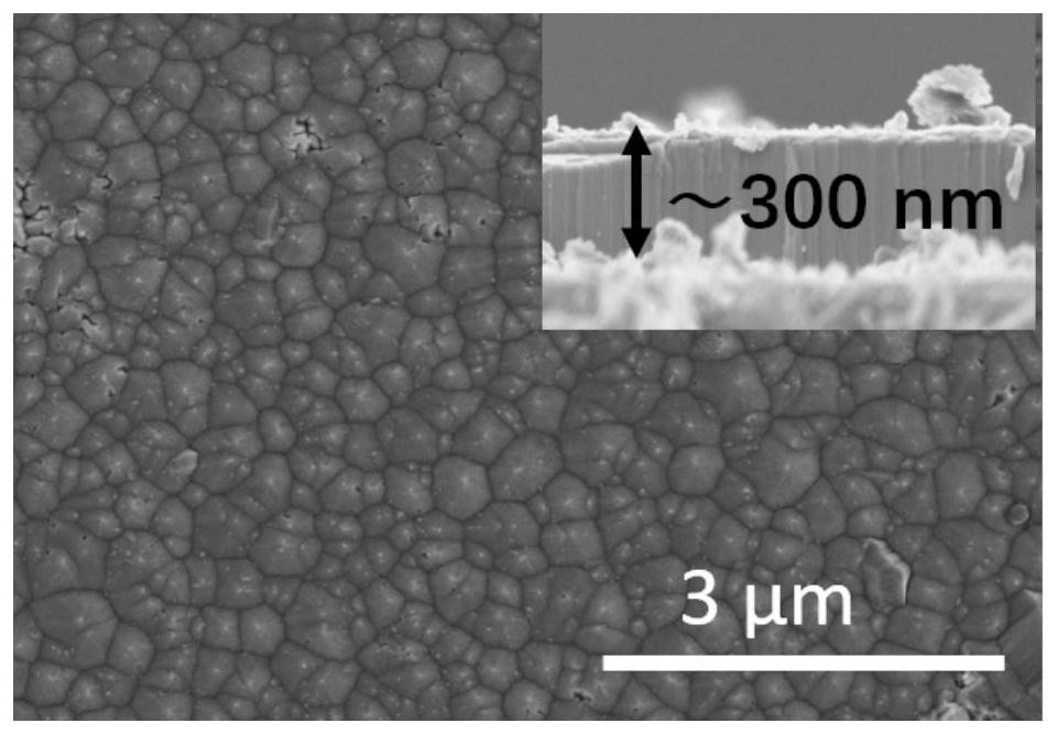
[0064] Put the prepared sample containing gold nanoparticles on the silicon plate heater in the deposition chamber of the pulse laser deposition instrument, use the mechanical pump to pump the deposition chamber to 2.0 Pa, then turn on the molecular pump to draw a high vacuum until the vacuum degree reaches 10 -4 When Pa is about, turn off the molecular pump; then pass a certain amount of oxygen into the deposition chamber, adjust the current of the silicon plate to slowly increase the temperature to 400°C, then focus the KrF excimer ...

Embodiment 2

[0069] The preparation process of the embodiment of the present invention is similar to that of embodiment 1, the difference is that when preparing aluminum nanoparticles by sputtering, the sputtering time is 24s; in addition, when configuring the dielectric microsphere suspension, the diameter is 1.5 μm transparent dielectric microspheres were mixed with ethanol at a concentration of 1×10 6 µL -1 .

[0070] Using 325nm ultraviolet excitation light to excite the film, the resulting 376nm wavelength luminous intensity a is 101 times that of the pure zinc oxide film luminous intensity b, the results are as follows Figure 8 shown.


PUM

PropertyMeasurementUnit
thicknessaaaaaaaaaa
thicknessaaaaaaaaaa
particle diameteraaaaaaaaaa

Abstract

The invention discloses a laminated structure capable of enhancing fluorescence light-emitting intensity of a light-emitting film and a preparation method thereof. The laminated structure comprises asingle-layer dielectric microsphere array, a light-emitting film and a substrate, which are in laminated connection in sequence. The laminated structure also comprises a first metal nanoparticle layerembedded between the light-emitting film and the substrate, and a second metal nanoparticle layer embedded between the light-emitting film and the single-layer dielectric microsphere array. The provided laminated structure capable of enhancing fluorescence light-emitting intensity of the light-emitting film combines combined actions of dielectric microsphere light field regulation and control andmetal surface plasmon coupling effect, and can make the fluorescence light-emitting intensity of the light-emitting film improve greatly; and such enhancing effect is far better than the enhancing effect obtained when the metal nanoparticle layer or the single-layer dielectric microsphere array is used separately. The structure is low in preparation cost, simple in process, short in process consumed time and is not limited by any substrate, and is suitable for light-emitting enhancement of the high-quality semiconductor light-emitting film.

Description

technical field [0001] The invention belongs to the technical field of luminescent materials, and relates to a lamination structure for enhancing the fluorescence luminous intensity of a luminescent thin film and a preparation method thereof. Background technique [0002] The third-generation semiconductor materials are widely used in blue, green, and purple light-emitting diodes and semiconductor lasers because of their large band gap, high electron drift saturation speed, and small dielectric constant; at the same time, semiconductor lighting has also become However, due to the low luminous intensity of some materials, it has become an obstacle to its practical application. Improving the luminous efficiency of materials is particularly important for large-scale applications in related fields. [0003] At present, the main methods for regulating the luminescence properties of semiconductor materials include metal surface plasmon coupling, laser irradiation, and doping; amon...

Claims


Application Information

Patent Timeline
Patent Type & Authority Patents(China)
IPC IPC(8): H01L33/50C23C14/16C23C14/18C23C14/34C23C14/08C23C14/35C23C14/28C23C28/00
CPCC23C14/086C23C14/165C23C14/185C23C14/28C23C14/34C23C14/35C23C28/30H01L33/502
Inventor 闫胤洲张玉洁蒋毅坚杨立学邢承
Owner BEIJING UNIV OF TECH
Learn More