Indium tin oxide/vertical graphene photoelectric detector composite structure and preparation method thereof

A photodetector, indium tin oxide technology, applied in the direction of circuits, electrical components, semiconductor devices, etc., can solve the problems of weak light absorption and low responsivity of single-layer graphene, and achieve good light transmittance and charge transport performance, Effect of multiple photocurrents and increased light absorption

Active Publication Date: 2019-10-15
BEIJING UNIV OF TECH
View PDF8 Cites 3 Cited by
  • Summary
  • Abstract
  • Description
  • Claims
  • Application Information

AI Technical Summary

Problems solved by technology

However, the photoresponsivity of current graphene photodetectors is at the level of several mA / W, and the main reason for the low responsivity is: the weak light absorption of single-layer graphene, and the carrier lifetime is on the order of ps

Method used


Image

  • Indium tin oxide/vertical graphene photoelectric detector composite structure and preparation method thereof
  • Indium tin oxide/vertical graphene photoelectric detector composite structure and preparation method thereof
  • Indium tin oxide/vertical graphene photoelectric detector composite structure and preparation method thereof

Examples


Embodiment 1

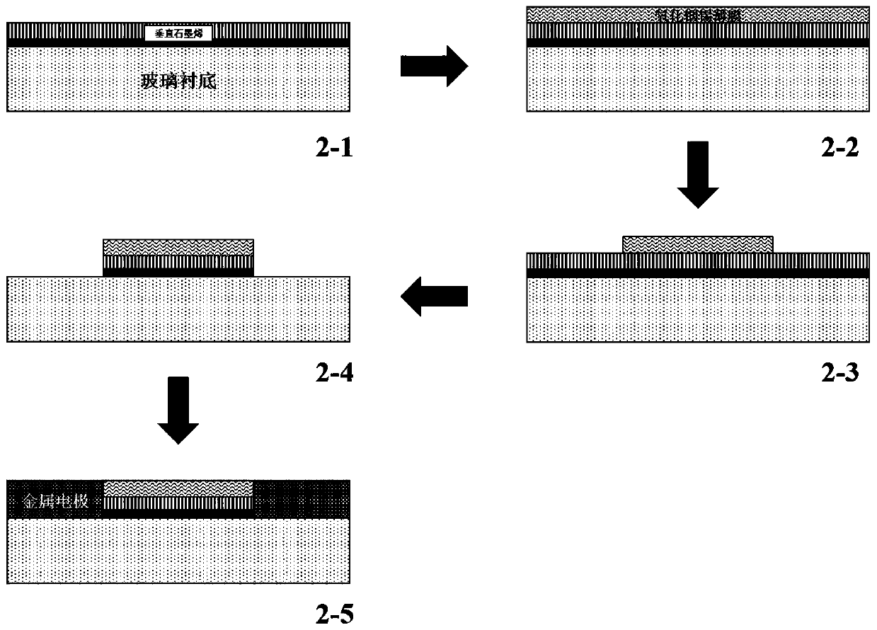
[0033] Embodiment 1: the preparation method of indium tin oxide / vertical graphene photodetector composite structure

[0034] Prepare indium tin oxide / vertical graphene photodetector composite structure, the preparation method step of the present invention is as follows:

[0035] (1) Directly grow vertical graphene on the glass substrate, the vertical graphene height is about 400nm (wherein the height of the buffer layer is much lower than the height of the graphene sheet, generally about 50nm), clean the vertical graphene sample: use acetone in turn solution, ethanol solution and deionized water to clean the vertical graphene sample;

[0036] (2) Preparation of indium tin oxide thin film: on vertical graphene grown on a glass substrate, a 100nm indium tin oxide thin film was deposited using magnetron sputtering technology, and the deposition temperature was 100°C;

[0037](3) Etching the indium tin oxide thin film channel: use AZ5214 photoresist, adopt the positive photolitho...

Embodiment 2

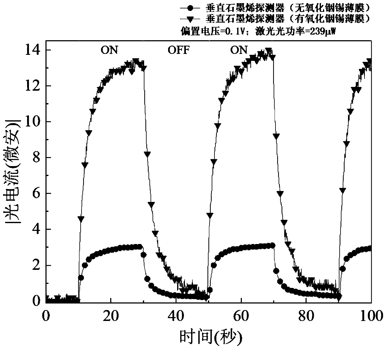
[0041] Embodiment 2: the photocurrent test (ie comparative example) of vertical graphene photodetector (no indium tin oxide thin film)

[0042] A vertical graphene photodetector (indium tin oxide-free thin film), the device structure includes: glass as the substrate of the device; vertical graphene as the light absorption layer and electron transport layer of the device; both sides of the vertical graphene are titanium / The gold electrodes are connected to an external power source. refer to image 3 The circular (●) curve in the figure was tested at room temperature and standard atmospheric pressure. A 980nm semiconductor pump laser was used as the test light source. The optical power of the light source was 239μW. Under the external bias voltage of 0.1V, the The generated photocurrent is 3.02μA, and the photoresponsivity is 12.6mA / W.

Embodiment 3

[0043] Embodiment 3: the photocurrent test of vertical graphene photodetector (with indium tin oxide thin film)

[0044] A vertical graphene photodetector (with indium tin oxide film), the device structure includes: glass as the substrate of the device; vertical graphene as the light absorption layer and electron transport layer of the device; the indium tin oxide film as the transparent current diffusion layer; on both sides of the vertical graphene are titanium / gold electrodes connected to an external power source. refer to image 3 The triangle (▼) curve in the figure is tested at room temperature and standard atmospheric pressure. A 980nm semiconductor pump laser is used as the test light source. The optical power of the light source is 239μW. Under the external bias voltage of 0.1V, the The photocurrent is 13.4μA, and the photoresponsivity is 56.1mA / W.

[0045] Show according to the experimental result of embodiment 2 and 3, the photoelectric current that the vertical g...


PUM

PropertyMeasurementUnit
thicknessaaaaaaaaaa
thicknessaaaaaaaaaa

Abstract

The invention provides an indium tin oxide/vertical graphene photoelectric detector composite structure and a preparation method thereof and belongs to the technical field of a photoelectric detector.The photoelectric detector comprises the following components from the bottom up in sequence: glass serving as a substrate of the device, vertical graphene serving as an optical absorption layer andan electron transport layer of the device, an ITO (indium tin oxide) thin film serving as a transparent current assisted diffusion layer, and titanium/gold electrodes arranged at the two sides of thevertical graphene and connected to an external power source. Since the vertical graphene has a broadband spectrum response characteristic, the detector operates in bands from the visible light band tothe infrared band; the designed ITO thin film can effectively transfer photo-induced carriers, thereby suppressing defect influence and improving output photocurrent of the device; besides, the detector has high light absorption rate and light response, and can work under a low bias voltage; the process is simple and repeatable; and detection efficiency and rate of finished product of the detector are improved effectively.

Description

technical field [0001] The invention belongs to the structure design and preparation method of a new material photodetector, in particular to a composite structure design and preparation method of an indium tin oxide / vertical graphene photodetector. Background technique [0002] A photodetector is a device that converts light signals into electrical signals. Light detection and photodetectors are of great significance in modern society, from imaging, communication equipment, security monitoring of various sensors, and display technology to basic Scientific applications, such as observing the universe. In general, an electronic transition should have at least two energy levels, and only incident photons with energy greater than the energy difference between these two levels can be absorbed. Therefore, semiconductor photodetectors, such as InGaAs-based infrared detectors and silicon-based photodetectors, have a limited detection wavelength range. However, graphene's zero-ban...

Claims


Application Information

Patent Timeline
Patent Type & Authority Applications(China)
IPC IPC(8): H01L31/0216H01L31/09H01L31/18
CPCH01L31/0216H01L31/09H01L31/1876Y02P70/50
Inventor 关宝璐杨嘉炜慈海娜刘忠范
Owner BEIJING UNIV OF TECH
Why Eureka
Try Eureka