Field effect transistor gas sensor and array preparation method thereof

A field effect transistor and gas sensor technology, applied in the field of semiconductor gas sensors, can solve problems such as phase transition, increase device power consumption, and limit low-power Internet of Things

Active Publication Date: 2019-12-17
HUAZHONG UNIV OF SCI & TECH
View PDF5 Cites 13 Cited by
  • Summary
  • Abstract
  • Description
  • Claims
  • Application Information

AI Technical Summary

Problems solved by technology

Patent CN2051351U discloses a "highly stable semiconductor hydrogen sensor", which is mainly composed of a hydrogen-sensitive Pd gate MOS device and heating resistors and other components for silicon-based integration to achieve highly stable and reliable hydrogen detection performance. However, the sensor requires heating assistance , which undoubtedly increases the power consumption of the device and limits the development of low-power IoT applications
Ali Javey et al. at the University of California, Berkeley used different metal materials (Pd, Ni, Au) as gates to construct FET array structures (Sci.Adv.2017,3(3),e1602557), which can selectively identify different gases , realizing the integration of multi-gas sensing units on a chip; how...

Method used


Image

  • Field effect transistor gas sensor and array preparation method thereof
  • Field effect transistor gas sensor and array preparation method thereof

Examples


preparation example Construction

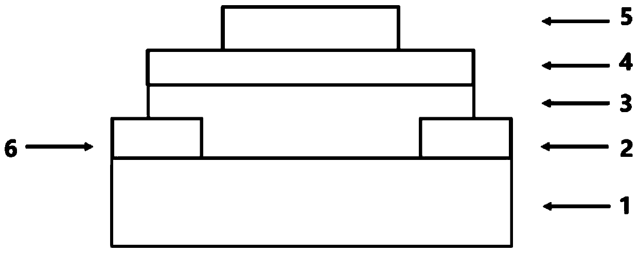
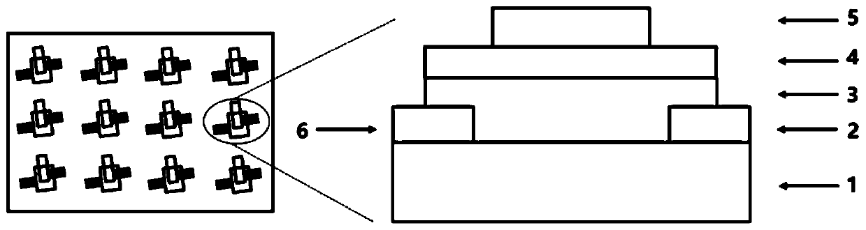
[0062] The preparation method of the grid-sensitive FET gas sensor can adopt the following steps: the quantum dot material is prepared by the colloidal method and dispersed in the liquid phase to form a colloidal quantum dot; 2 or Si / Si 3 N 4 Micro-nano electrode patterns are formed on commercial substrates through process steps such as photolithography masks, and then Ti / Au composite layers or Cr / Au composite layers or Ni / Au composite layers are deposited by physical methods such as electron beam evaporation, thermal evaporation, and magnetron sputtering Combined layer forms source, drain electrode (drain electrode and the composition material of source electrode both can be identical, for example can all be Ti / Au layer, can pass through photolithography mask at this moment, the source drain electrode of physical method deposition gained; Of course Also can be different from each other, at this moment, need pass through twice photolithography mask, physical method deposition...

Embodiment 1

[0069] This embodiment comprises the following steps:

[0070] (1) Preparation of PbS colloidal quantum dot solution. PbO can be used as the lead source, and hexamethyldisilathane (TMS) can be used as the sulfur source, which can be produced by colloid chemical reaction.

[0071] Specifically, 0.9 g of PbO can be dissolved in 5 ml of oleic acid (OA) and 20 ml of octadecene (ODE) under a nitrogen atmosphere and heated to 90° C. to prepare a precursor of lead oleate as a lead source. After evacuating for 8 hours, the temperature of the precursor was raised to 120°C. Dissolve 280 μl TMS into 10 ml ODE as a sulfur source. Quickly inject the sulfur source into the lead source at 120°C, and after the color of the reaction system turns black (about 15 seconds), put the solution into cold water to quickly drop the temperature to room temperature. Add an appropriate amount of acetone to the cooled solution, remove the supernatant after centrifugation, and then disperse with toluene ...

Embodiment 2

[0079] (1) Preparation of SnO 2 Colloidal quantum dot solution. SnCl can be used 4 ·5H 2 O was used as the tin source, and oleic acid and oleylamine long-chain organic ligands were used as encapsulating agents, which were generated by solvothermal reaction.

[0080] Specifically, 0.6g SnCl can be 4 ·5H 2 O. 20ml of oleic acid and 2.5ml of oleylamine were heated to 100°C and vacuum-dried until the reaction was clear, cooled to 60°C, taken out 10ml of ethanol and mixed evenly, then added to a stainless steel autoclave, and placed in an oven at 180°C for 3 hours. After the reaction is completed, take it out, and when it is cooled to room temperature, take out the solution in the autoclave, mix it with ethanol and centrifuge the precipitate, then disperse the precipitated product in the solvent and perform ethanol centrifugation and washing again. After drying, disperse in toluene at a concentration of 20mg / ml to obtain SnO 2 Colloidal quantum dot solution.

[0081] (2) The...


PUM

PropertyMeasurementUnit
Thicknessaaaaaaaaaa
Thicknessaaaaaaaaaa
Particle sizeaaaaaaaaaa

Abstract

The invention discloses a field effect transistor gas sensor and an array preparation method thereof. The field effect transistor (FET) gas sensor is a gate-sensitive FET gas sensor with a gate electrode modified by quantum dots, and a gate-sensitive electrode layer (5) of the FET gas sensor is of a two-layer composite structure or of a single-layer structure made of a composite material. The two-layer composite structure comprises a metal film layer and a quantum dot layer deposited on the surface of the metal film layer. The single-layer structure made of a composite material is specificallya single-layer structure made of a composite material formed by combining quantum dots and a metal or metalloid material. According to the invention, improvement is made on the internal composition and structure of the gate-sensitive FET, the corresponding preparation method and the like, quantum dots are used as a gate electrode and a gas sensitive layer at the same time, and the bias voltage ofthe gate electrode and the channel modulation effect are regulated and controlled by utilizing the adsorption characteristic of a quantum dot gate-sensitive electrode to different gases. A room-temperature gas sensor with high sensitivity, low power consumption and high selectivity can be obtained, and low-concentration target gases (such as H2) can be detected.

Description

technical field [0001] The invention belongs to the technical field of semiconductor gas sensors, and more specifically relates to a field effect transistor gas sensor and a preparation method thereof. The gas sensor uses quantum dots as a field effect transistor (FET) ) gas sensor is a gate sensitive FET gas sensor. Background technique [0002] Gas sensors are one of the most effective ways to obtain gas information in real time and in situ, and play an irreplaceable and important role in environmental protection, security alarm and other fields. At present, gas sensors are limited by sensitivity, integration and power consumption, and it is difficult to improve the applicability and reliability of multi-component complex atmosphere environments. Gas sensors based on field effect transistors (FETs) can operate under low current and low voltage conditions, which is conducive to the integration of silicon-based arrays, and has become one of the research hotspots in the fiel...

Claims


Application Information

Patent Timeline
IPC IPC(8): G01N27/414
CPCG01N27/4141G01N27/4146G01N27/4148
Inventor 刘欢唐江李华曜刘竞尧严棋田枝来臧剑锋张建兵
Owner HUAZHONG UNIV OF SCI & TECH
Why Eureka
Try Eureka