
Method and device for rapidly filling vertical TSV hole with liquid alloy

A filling method, liquid alloy technology, applied in gaseous chemical plating, metal material coating process, semiconductor/solid-state device manufacturing, etc., can solve the problem of toxic electrolytes and additives, hours to tens of hours, and low filling efficiency, etc. problems, to achieve the effect of improving wettability, improving production efficiency, and fast filling process

Active Publication Date: 2020-02-14
BEIJING UNIV OF TECH
View PDF7 Cites 3 Cited by
  • Summary
  • Abstract
  • Description
  • Claims
  • Application Information

AI Technical Summary

Problems solved by technology

Due to its high aspect ratio structure, the copper electroplating process generally takes several hours to tens of hours, the filling efficiency is low, and the electrolyte and additives are toxic and pollute the environment
[0004] There is an urgent need for a new filling method to solve this problem. At present, most of them change the electroplating process parameters to reduce the defects in the filling process, but the problems of long time consumption and high production cost have not been solved.

Method used


Image

  • Method and device for rapidly filling vertical TSV hole with liquid alloy
  • Method and device for rapidly filling vertical TSV hole with liquid alloy
  • Method and device for rapidly filling vertical TSV hole with liquid alloy

Examples


Embodiment 1

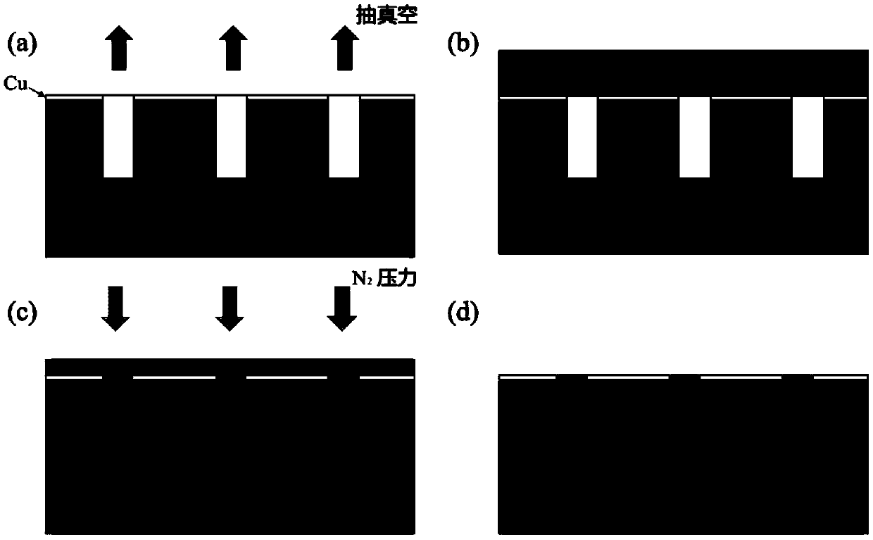
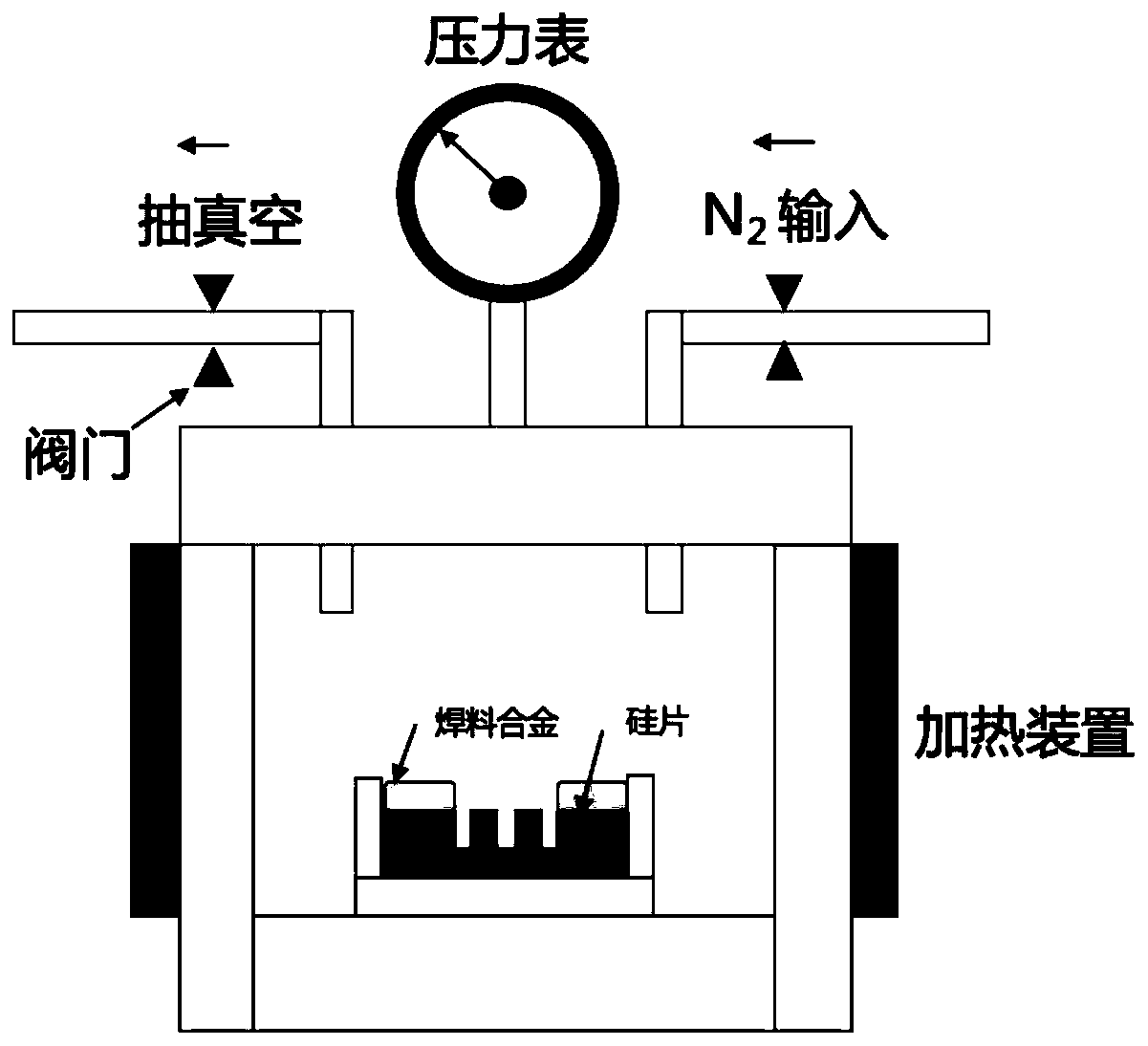
[0038] The alloy provided by the present invention fills the fast filling device of TSV, such as image 3 As shown, sealed reaction chamber, vacuum pump, nitrogen input device, vacuum outlet control valve, nitrogen inlet control valve, filling tank, heating device, temperature sensor.

Embodiment 2

[0040] The TSV fast filling method provided in this embodiment includes the following steps:

[0041] Step 1: The sample selected in this example is a copper-plated TSV blind hole silicon wafer with a diameter of 10 μm, a depth of 100 μm, and an aspect ratio of 10. The silicon wafer is cut into small pieces of 5mm*5mm by laser, and the cut out small pieces into 20% HNO 3 Soak in the solution for 20s, then take it out with tweezers, put it into a beaker filled with absolute ethanol, and clean it with an ultrasonic cleaner for 10 minutes.

[0042] Step 2: Polish the Sn3.0Ag0.5Cu solder alloy with sandpaper to remove the surface oxide film, then put it into a beaker filled with absolute ethanol and ultrasonically clean it to remove surface impurities and then dry it

[0043] Step 3: Place the sample tank containing the solder alloy and the sample in the reaction chamber of the filling device, and seal the reaction chamber. At this time, the valves at the vacuum outlet and the ni...


PUM


Abstract

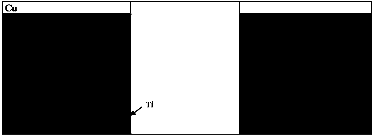
The invention provides a method and device for rapidly filling a vertical TSV hole with liquid alloy, and relates to the field of microelectronic packaging. With solder alloy as a filling material, asilicon dioxide insulation layer is deposited on the surface of a TSV silicon wafer and in a blind hole in advance through chemical vapor deposition, a titanium barrier layer is deposited on the wallof the hole through physical vapor deposition, and finally, a copper layer is electroplated on the surface of the silicon wafer deposited with silicon dioxide to serve as a wet layer; and the obtainedwafer is placed in a vacuum chamber, the alloy is heated to be molten, the silicon wafer is pressurized when completely making contact with the molten alloy due to the wettability of the solder alloyand copper, the pressure in the vacuum chamber is maintained after pressurization, and filling is completed after the temperature is decreased. By the adoption of the method and device, the filling efficiency of the TSV hole can be improved, and imporous filling of a high-depth-wide-ratio TSV blind hole with the solder alloy is completed. The alloy and the wall of the TSV hole are firmly bonded together, and the filling process is simple. The TSV hole filling device comprises a vacuum outlet, a nitrogen inlet, a pressure gauge, a reaction chamber, a heating device and a temperature display device, wherein the vacuum outlet and the nitrogen inlet are controlled through valves.

Description

technical field [0001] The invention relates to the technical field of microelectronic packaging, in particular to a method and a device for rapidly filling a through-silicon hole with an alloy. Background technique [0002] Moore's law has been guiding the development direction of electronic information technology since 1965. However, with the emergence of smaller line width technology, people realize that it is becoming more and more important to integrate higher density circuits and realize more functions on a single chip. Difficulties, three-dimensional integrated packaging technology is considered to be the preferred solution to achieve device miniaturization and multi-function, and through silicon via (Through Silicon Via, TSV) technology is the core of three-dimensional integrated packaging technology, TSV technology can realize the interconnection between stacked chips Vertically interconnected up and down, this structure can play the role of signal conduction and he...

Claims


Application Information

Patent Timeline
Patent Type & Authority Applications(China)
IPC IPC(8): C23C16/40C23C14/16C25D7/12C25D3/38C25D5/48H01L21/768
CPCC23C14/16C23C16/402C25D3/38C25D5/48C25D7/12H01L21/76814H01L21/76898
Inventor 马立民冯剑雨王乙舒郭福
Owner BEIJING UNIV OF TECH
Learn More