Vanadium dioxide and two-dimensional semiconductor junction type photodetector and preparation method thereof

A two-dimensional semiconductor, vanadium dioxide technology, applied in the field of nanomaterials, can solve the problems of limited absorption, difficult to extend, difficult to suppress, etc., to achieve the effect of reducing self-resistance, changing current size, and high-sensitivity photodetection

Pending Publication Date: 2020-05-08
SHANGHAI INST OF TECHNICAL PHYSICS - CHINESE ACAD OF SCI
View PDF0 Cites 6 Cited by
  • Summary
  • Abstract
  • Description
  • Claims
  • Application Information

AI Technical Summary

Problems solved by technology

[0003] However, transition metal chalcogenides are not all smooth sailing in the field of photodetection. For example, its band gap limits its application in infrared photodetectors, because the band gap of this type of semiconductor itself falls in the ultraviolet to visible band, although It can be extended to the near-infrared band through energy band engineering [Advanced Materials 27, 6575 (2015)], but it is difficult to extend it further
Although there are other two-dimensional semiconductors, such as Bi 2 SeO 2 [NatureCommunications 9,3311(2018)] and BP[Nature Nanotechnology 10,707(2015)], the bandgap width of these materials can be adjusted, and the bandgap can be controlled at 0.2-0.3eV through thickness control, which can correspond to mid-wave infrared area, but the difficulty of preparation and air stability of these materials have inhibited their development
In addition, the thickness of two-dimensional materials also limits its absorption of light, resulting in low photoelectric conversion efficiency, and thick two-dimensional materials have a large dark current, which is difficult to be completely suppressed

Method used


Image

  • Vanadium dioxide and two-dimensional semiconductor junction type photodetector and preparation method thereof
  • Vanadium dioxide and two-dimensional semiconductor junction type photodetector and preparation method thereof
  • Vanadium dioxide and two-dimensional semiconductor junction type photodetector and preparation method thereof

Examples


Embodiment 1

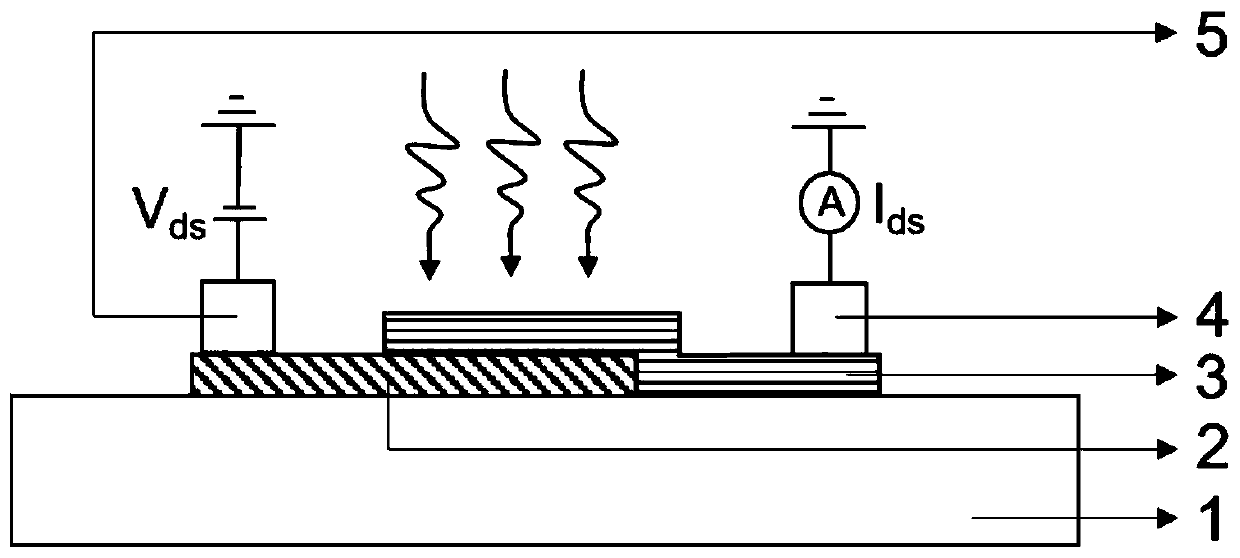
[0023] 1) A uniform vanadium metal film is sputtered on an alumina substrate by magnetron sputtering, and transformed into a vanadium dioxide film by thermal oxidation, with a film thickness of 22 nanometers and a surface roughness of 1 nanometer ;

[0024] 2) using ultraviolet lithography to make an array mask on the vanadium dioxide film in step 1, using argon plasma etching technology to etch away the exposure area, and forming a square array of vanadium dioxide after removing the mask;

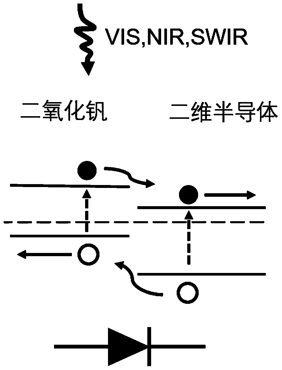
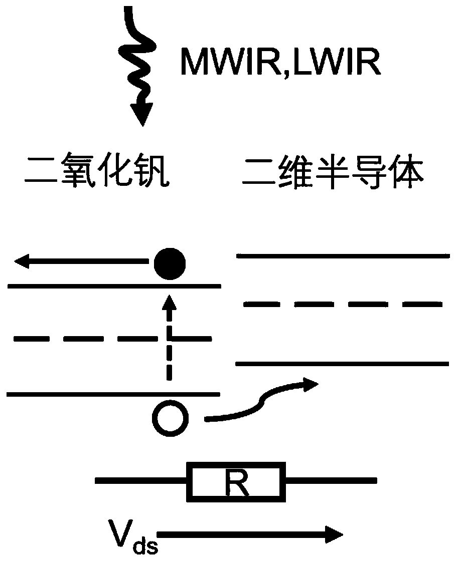
[0025] 3) The two-dimensional semiconductor molybdenum ditelluride is peeled off on the silicon wafer by a mechanical peeling method, with a thickness of 20 nanometers. Use polydimethylsiloxane (PDMS) to transfer the exfoliated two-dimensional semiconductor to the surface of vanadium dioxide in step 2, and then remove PDMS to form a vertical heterojunction structure of two-dimensional semiconductor material and vanadium dioxide dislocation stacking .

[0026] 4) Using ultraviolet lithogr...

Embodiment 2

[0028] 1) A uniform vanadium metal film is sputtered on an alumina substrate by magnetron sputtering, and transformed into a vanadium dioxide film by thermal oxidation, with a film thickness of 22 nanometers and a surface roughness of 1 nanometer ;

[0029] 2) using ultraviolet lithography to make an array mask on the vanadium dioxide film in step 1, using argon plasma etching technology to etch away the exposure area, and forming a square array of vanadium dioxide after removing the mask;

[0030] 3) The two-dimensional semiconductor molybdenum ditelluride is peeled off on the silicon wafer by a mechanical peeling method, with a thickness of 30 nanometers. Use polydimethylsiloxane (PDMS) to transfer the exfoliated two-dimensional semiconductor to the surface of vanadium dioxide in step 2, and then remove PDMS to form a vertical heterojunction structure of two-dimensional semiconductor material and vanadium dioxide dislocation stacking .

[0031] 4) Using ultraviolet lithogr...

Embodiment 3

[0033] 1) A uniform vanadium metal film is sputtered on an alumina substrate by magnetron sputtering, and transformed into a vanadium dioxide film by thermal oxidation, with a film thickness of 22 nanometers and a surface roughness of 1 nanometer ;

[0034] 2) using ultraviolet lithography to make an array mask on the vanadium dioxide film in step 1, using argon plasma etching technology to etch away the exposure area, and forming a square array of vanadium dioxide after removing the mask;

[0035] 3) The two-dimensional semiconductor molybdenum ditelluride is peeled off on the silicon wafer by a mechanical peeling method, with a thickness of 40 nanometers. Use polydimethylsiloxane (PDMS) to transfer the exfoliated two-dimensional semiconductor to the surface of vanadium dioxide in step 2, and then remove PDMS to form a vertical heterojunction structure of two-dimensional semiconductor material and vanadium dioxide dislocation stacking .

[0036] 4) Using ultraviolet lithogr...


PUM

PropertyMeasurementUnit
thicknessaaaaaaaaaa
surface roughnessaaaaaaaaaa
thicknessaaaaaaaaaa

Abstract

The invention discloses a vanadium dioxide and two-dimensional semiconductor junction type photodetector and a preparation method thereof. According to the photodetector, the method comprises the steps of: growing a layer of uniform vanadium dioxide film on an aluminum oxide substrate through magnetron sputtering; etching the vanadium dioxide film into an array by using a photoetching mask and anargon plasma etching technology; and transferring the two-dimensional semiconductor to a vanadium dioxide material through dry transfer to form a heterojunction with a vertical structure, and preparing a metal electrode on the vanadium dioxide and the two-dimensional semiconductor by using an electron beam lithography method in combination with a stripping process to form the heterojunction type optical detection device with the vertical structure. The device structurally comprises the substrate, vanadium dioxide, the two-dimensional semiconductor and metal source and drain electrodes from bottom to top. By regulating and controlling bias voltage, the device can realize P-N junction and Bolometer conversion, thereby realizing detection from visible light to far infrared band spectrum, being low in power consumption and high in sensitivity, and being capable of working in a high-temperature environment.

Description

technical field [0001] The invention relates to a junction photodetection device of vanadium dioxide and two-dimensional semiconductor, belonging to the technical field of nanometer materials. Background technique [0002] In recent years, molybdenum disulfide (MoS 2 ) The emergence of transition metal chalcogenides, represented by , provides an opportunity for the development of the field of photodetection. This type of transition metal chalcogenide [Nature Nanotechnology 7,699(2012)] has a band gap of 1eV-2eV, and the effective carrier mobility can be as high as hundreds of cm 2 V -1 the s -1 , and can be prepared in a large area by chemical vapor deposition. These excellent properties make this type of material suitable for effective detection of visible light. In fact, photodetectors based on two-dimensional semiconductors have already been studied and have achieved good development. For example, photodetectors based on molybdenum disulfide [Nature Nanotechnology 8,4...

Claims


Application Information

Patent Timeline
Patent Type & Authority Applications(China)
IPC IPC(8): H01L31/0336H01L31/0352H01L31/108H01L31/109H01L31/18
CPCH01L31/0336H01L31/035272H01L31/108H01L31/109H01L31/18Y02P70/50
Inventor 王建禄蒋伟孟祥建沈宏林铁褚君浩
Owner SHANGHAI INST OF TECHNICAL PHYSICS - CHINESE ACAD OF SCI
Why Eureka
Try Eureka