Mask structure of copper electroplating grid line for HAC battery and preparation method of mask structure
A technology of copper electroplating and masking, which is applied in the manufacture of circuits, electrical components, and final products, can solve the problem that the anti-reflection effect cannot be optimal, achieve suitable scale production, improve the anti-reflection effect, and save a lot of cost Effect
- Summary
- Abstract
- Description
- Claims
- Application Information
AI Technical Summary
Problems solved by technology
Method used
Image

Examples
Embodiment 1
[0024] Embodiment 1 silicon nitride as mask layer
[0025] Deposit a layer of ITO film on both surfaces of the crystalline silicon wafer deposited with amorphous silicon as the TCO layer, and then use the plate PECVD method to deposit a layer of silicon nitride on each of the two ITO film surfaces as the copper plating grid line. Mask layer; the mask is slotted by placing a hard mask on the surface of the cell during coating;
[0026] When the silicon nitride film is deposited, a solid-state mask is used to form a thin grid line pattern with a line width of 40 μm and a line spacing of 400 μm. The thin grid line is prepared by electroplating. The thickness of the copper electroplating grid line is 0.2-20 μm. The preparation process Discontinuity is allowed in the copper plating grid line;
[0027] The silicon nitride mask layer remains on the surface of the battery sheet after the preparation of the copper electroplating grid lines, and is not removed.
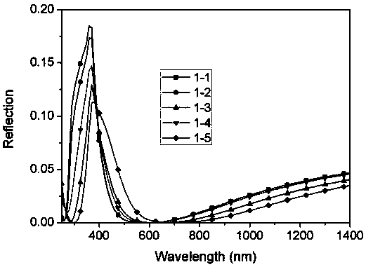
[0028] Several groups...
Embodiment 2
[0033] Embodiment 2 silicon oxide as mask layer
[0034] Deposit a layer of ITO film on both surfaces of the crystalline silicon wafer deposited with amorphous silicon as the TCO layer, and then use the plate PECVD method to deposit a layer of silicon oxide on each of the two ITO film surfaces as a mask for the copper electroplating gate line. The film layer; and after the coating is finished, the mask is notched by etching with an etchant;
[0035] After the deposition of the silicon oxide film, the silicon oxide etchant is printed by screen printing to etch the silicon oxide film. In this process, only the mask material is etched and the TCO material is not etched, forming a line width of 30 μm and a line spacing of 1 mm. The thin grid line pattern and the main grid line pattern with a line width of 1.0 mm are prepared by electroplating. The thickness of the copper electroplating grid line is 0.2-20 μm, and the copper electroplating grid line is allowed to have discontinuity...
Embodiment 3
[0042] Embodiment 3 silicon nitride-silicon oxide as mask layer
[0043] Deposit one layer of ITO film on the two surfaces of the crystalline silicon wafer deposited with amorphous silicon as the TCO layer, and then use the hot wire CVD method to deposit a layer of silicon nitride film on the two ITO film surfaces, and then separately Deposit a layer of silicon oxide film as a mask layer for copper electroplating gate lines;
[0044] After the film deposition, the silicon oxide etchant was printed by screen printing to etch the silicon oxide film to form a fine grid line pattern with a line width of 10 μm and a line spacing of 1 mm, and a main grid line pattern with a line width of 1.0 mm. , using the electroplating method to prepare fine grid lines, the thickness of the copper electroplated grid lines is 0.2-20 μm, and the copper electroplated grid lines are allowed to be discontinuous during the preparation process;
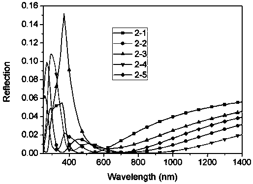
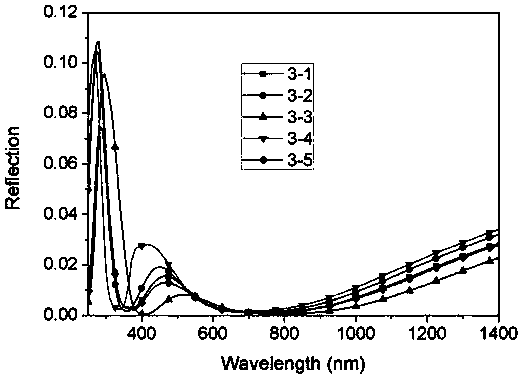
[0045] Several groups of example samples were analyzed, ...
PUM
| Property | Measurement | Unit |
|---|---|---|
| Thickness | aaaaa | aaaaa |
| Thickness | aaaaa | aaaaa |
| Thickness | aaaaa | aaaaa |
Abstract
Description
Claims
Application Information
 - R&D
- Intellectual Property
- Life Sciences
- Materials
- Tech Scout
- Unparalleled Data Quality
- Higher Quality Content
- 60% Fewer Hallucinations
Browse by: Latest US Patents, China's latest patents, Technical Efficacy Thesaurus, Application Domain, Technology Topic, Popular Technical Reports.
© 2025 PatSnap. All rights reserved.Legal|Privacy policy|Modern Slavery Act Transparency Statement|Sitemap|About US| Contact US: help@patsnap.com