Three-dimensional integrated millimeter wave AiP phased array element

A three-dimensional integration, millimeter-wave technology, applied in the direction of electrical components, antenna arrays, radiation element structure, etc., can solve the problems of low energy efficiency, backward packaging structure, high power consumption, etc., to achieve controllable collapse height, high integration, and low loss low effect

Active Publication Date: 2020-06-12
南京国微电子有限公司
View PDF11 Cites 14 Cited by
  • Summary
  • Abstract
  • Description
  • Claims
  • Application Information

AI Technical Summary

Problems solved by technology

Among them, microwave chips, digital chips and PCB substrates adopt the traditional gold wire bonding method, which makes the insertion loss high and the standing wave coefficient deteriorate significantly in the millimeter wave frequency band
The discrete antenna and the millimeter-wave front-end are electrically interconnected through traditional connectors such as coaxial cables, SMA, and SMP, which have the disadvantages of large size and weight, and high power consumption, which limits the use of millimeter-wave radar in mobile terminals, the Internet of Things, Used in devices with high miniaturization requirements such as Internet of Vehicles
[0004] It can be seen from the above that the existing technology has the following problems: the millimeter-wave AiP phased array element is large in size, low in energy efficiency, serious in millimeter-wave loss, and the packaging structure is backward, which cannot meet the requirements of miniaturization and low cost.

Method used


Image

  • Three-dimensional integrated millimeter wave AiP phased array element
  • Three-dimensional integrated millimeter wave AiP phased array element
  • Three-dimensional integrated millimeter wave AiP phased array element

Examples


Embodiment 1

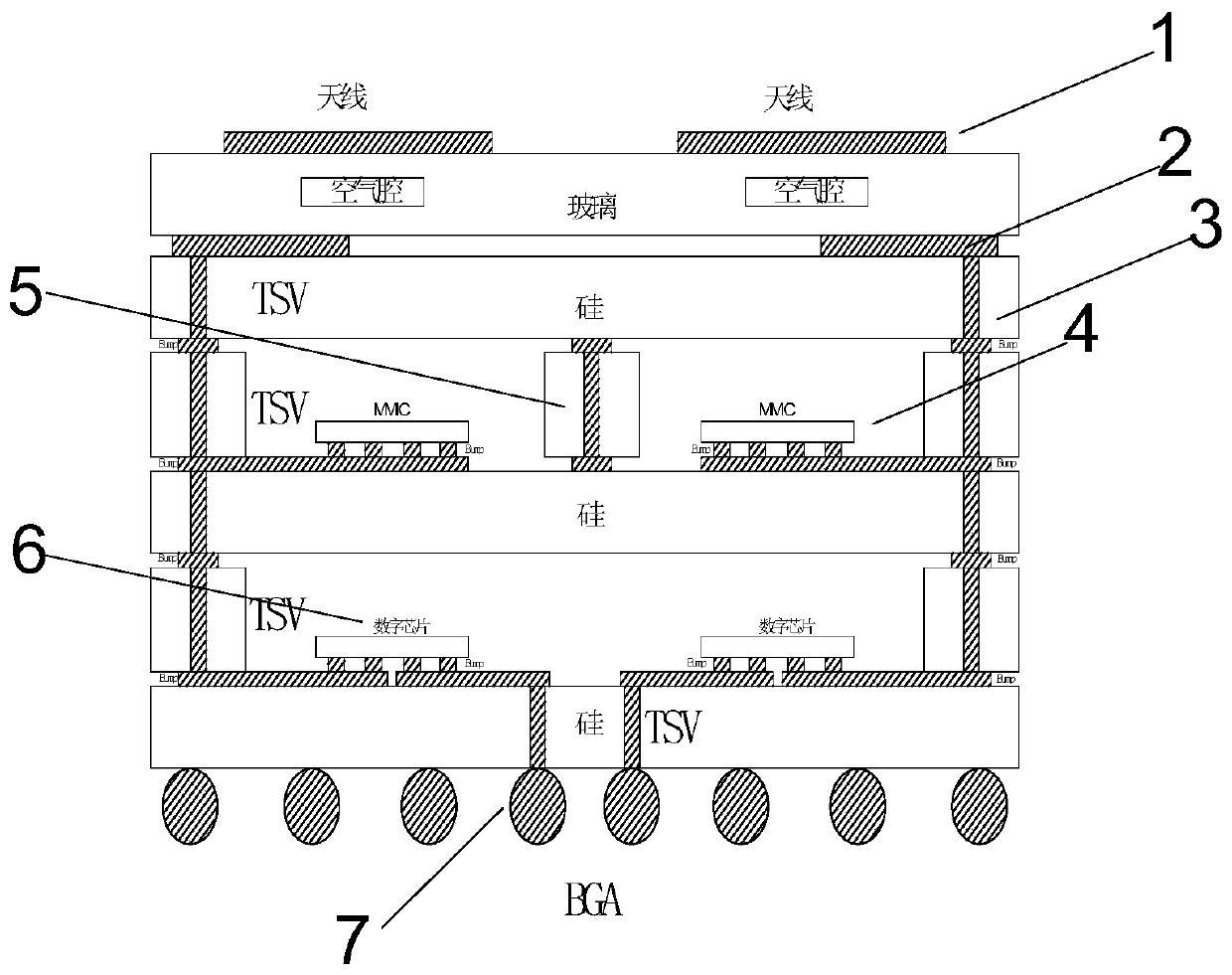
[0040] combine figure 1 , a three-dimensional integrated millimeter-wave AiP phased array element of the present invention uses a combination of silicon-based semiconductor packaging technology and glass-based micro-nano processing technology to vertically interconnect the millimeter-wave antenna and multilayer functional circuits in the Z-axis direction . From top to bottom: millimeter wave microstrip patch antenna array layer 1, antenna feed network layer 2, millimeter wave signal transmitting and receiving circuit layer 3, millimeter wave signal three-dimensional vertical transmission layer 4, millimeter wave circuit shielding layer 5 , Power division network and digital signal layer 6 and bottom BGA signal input layer 7.

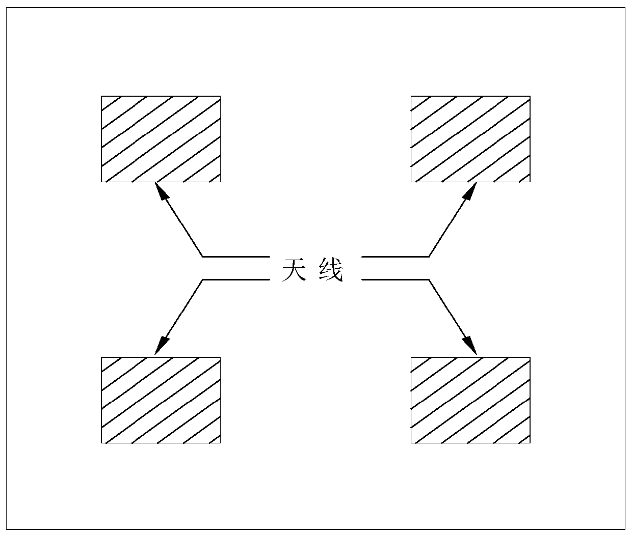
[0041] Such as figure 2 As shown, the number of millimeter-wave microstrip patch antenna elements is N×N, N≥2, and glass with low loss and low dielectric constant is used as the radiation substrate. The glass micro-nano processing technology includes ...

Embodiment 2

[0049] Such as figure 1 As shown, a new three-dimensional integrated millimeter-wave AiP phased array element, its design architecture includes high-gain millimeter-wave microstrip antenna array, antenna feed network, millimeter-wave signal transmitting and receiving circuit, three-dimensional vertical transmission circuit, different channels Shielding design, power division network and digital chip circuit and fine-pitch BGA port design.

[0050] Such as figure 2 As shown, the millimeter-wave microstrip patch antenna array is formed by 2×2=4 glass-based radiating elements. The array is a rectangular square array, and the feeding mode of space coupling is adopted. The air cavity is etched on the glass substrate by laser to realize the high gain, high efficiency and high bandwidth of the 2×2 rectangular antenna array. The glass with cavity and the glass with pattern metallization are bonded together by wafer-level bonding. The antenna and the feed are interconnected using a...


PUM


Abstract

The invention discloses a three-dimensional integrated millimeter wave AiP phased array element. A millimeter wave microstrip patch antenna array layer, an antenna feed network layer, a millimeter wave signal transmitting and receiving circuit layer, a millimeter wave signal three-dimensional vertical transmission layer, a millimeter wave circuit shielding layer, a power division network and digital signal layer and a bottom BGA signal input layer are sequentially arranged from the top layer to the bottom layer. According to the invention, a silicon semiconductor integrated packaging process and a glass wiring process are adopted, passive devices such as a millimeter wave microstrip patch antenna, a feed network, a microwave chip, a digital chip, an IPD and the like are packaged into a miniaturized three-dimensional integrated millimeter wave AiP phased array element, and input and interlayer vertical transmission of millimeter wave signals are realized by utilizing high-density integrated BGA, TSV and Bump.

Description

technical field [0001] The invention relates to millimeter wave radar communication technology, in particular to a three-dimensional integrated millimeter wave AiP phased array element. Background technique [0002] With millimeter wave communication equipment, the demand for miniaturization, low profile and light weight of active phased array radar is increasing day by day. Due to its strong anti-interference ability, millimeter wave radar can penetrate plastics and ceramics, and its imaging resolution is high. With the characteristics of large data transmission bandwidth and other characteristics, it has begun to be used in large quantities in the civilian field. The millimeter-wave AiP (Antenna in Package) array element is a technology that integrates the antenna and chip into the package to realize system-level wireless functions based on packaging materials and processes. AiP technology conforms to the trend of increasing integration of silicon-based semiconductor proc...

Claims


Application Information

Patent Timeline
Patent Type & Authority Applications(China)
IPC IPC(8): H01Q1/22H01Q1/38H01Q1/50H01Q21/00H01Q21/06G01S7/02
CPCG01S7/02H01Q1/2283H01Q1/38H01Q1/50H01Q21/0006H01Q21/065
Inventor 沈国策周骏师建行杨东升杨驾鹏
Owner 南京国微电子有限公司
Why Eureka
Try Eureka