High-sensitivity negative capacitance field effect transistor photoelectric detector and preparation method

A technology of photodetectors and capacitive fields, applied in circuits, electrical components, semiconductor devices, etc., can solve problems such as large dark current, complex preparation process of quantum dot material size and quality control, low detection rate, etc. current, improve photodetection efficiency, and suppress dark current

Active Publication Date: 2020-06-19
SHANGHAI INST OF TECHNICAL PHYSICS - CHINESE ACAD OF SCI
View PDF5 Cites 9 Cited by
  • Summary
  • Abstract
  • Description
  • Claims
  • Application Information

AI Technical Summary

Problems solved by technology

Although molybdenum disulfide and mercury telluride quantum dot composite photodetectors can improve the above problems, the size and quality control of quantum dot materials and the complex preparation process still face many challenges
In addition, molybdenum disulfide photodetectors based on organic dye molecules or perovskite light-absorbing layers exhibit enhanced photoresponsivity, but the characteristic absorption spectra of low-dimensional materials are usually affected, and leakage channels are inevitably introduced, leading to Large dark current and low detection rate

Method used


Image

  • High-sensitivity negative capacitance field effect transistor photoelectric detector and preparation method
  • High-sensitivity negative capacitance field effect transistor photoelectric detector and preparation method
  • High-sensitivity negative capacitance field effect transistor photoelectric detector and preparation method

Examples


Embodiment 1

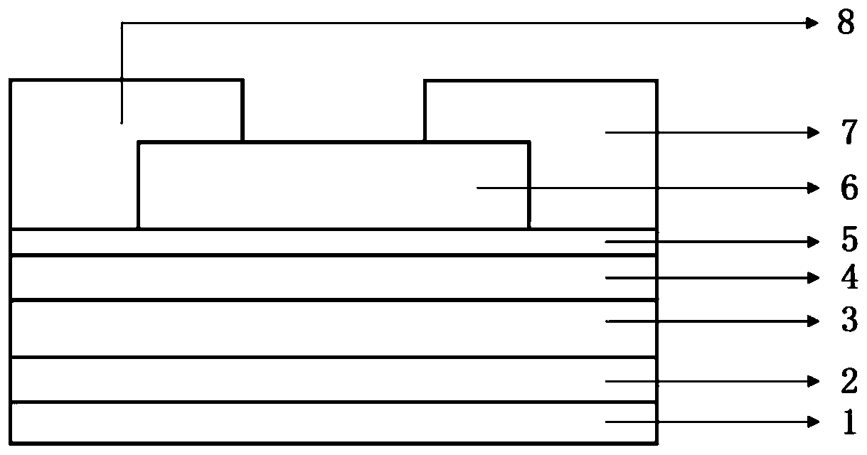
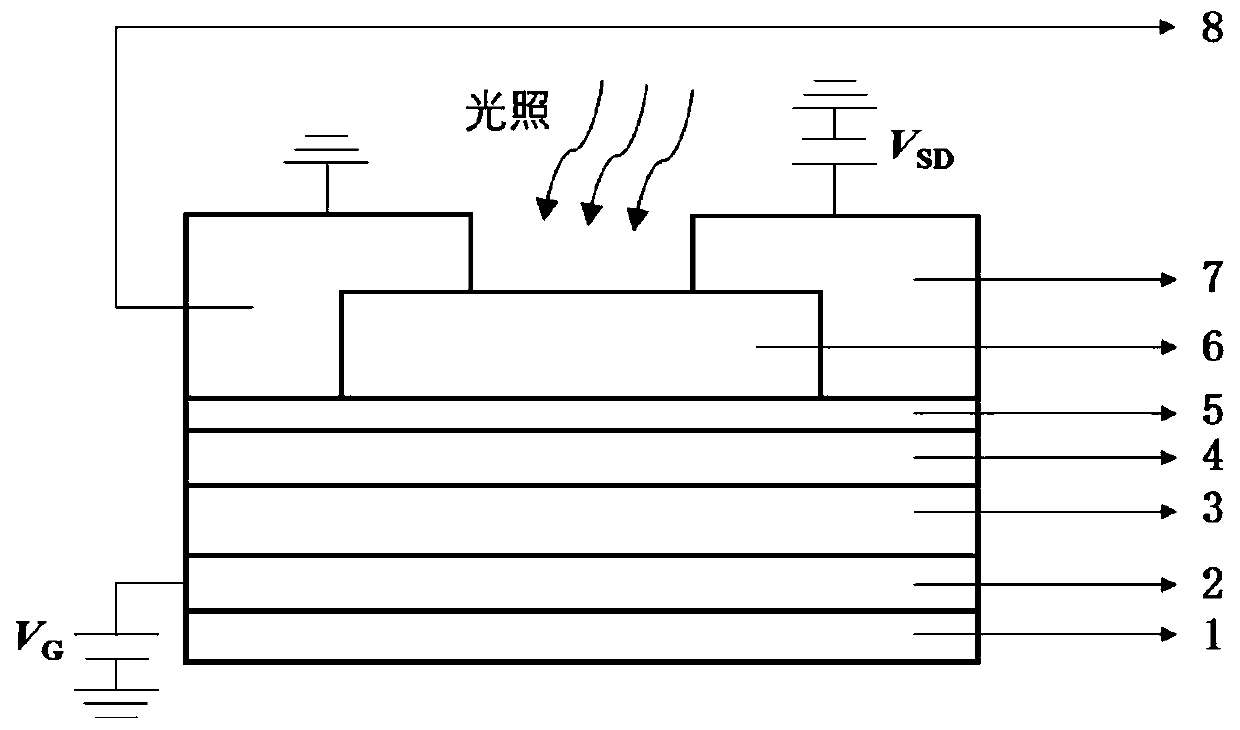
[0064] In this embodiment, a low-dimensional material phototransistor device under the control of a hafnium oxide-based ferroelectric film is provided. The cross-sectional view of the device is as follows figure 1 shown.

[0065] From bottom to top, the detector is as follows: 1 substrate, 2 oxide, 3 gate electrode, 4 hafnium oxide-based ferroelectric gate dielectric with negative capacitance effect, 5 oxide gate dielectric, 6 low-dimensional semiconductor material, 7 metal source electrodes with 8 metal drain electrodes.

[0066] In this embodiment, substrate 1 is a P-type doped silicon substrate; oxide layer 2 is silicon dioxide with a thickness of 285 nanometers; gate electrode 3 is titanium nitride with a thickness of 40 nanometers; hafnium oxide with negative capacitance effect The base ferroelectric grid dielectric 4 is zirconium-doped hafnium oxide, and the molecular formula is Hf 0.5 Zr 0.5 o 2 , with a thickness of 10 nanometers; the oxide gate dielectric 5 is alu...

Embodiment 2

[0071] In this embodiment, a low-dimensional material phototransistor device under the control of a hafnium oxide-based ferroelectric film is provided. The cross-sectional view of the device is as follows figure 1 shown.

[0072] From bottom to top, the detector is as follows: 1 substrate, 2 oxide, 3 gate electrode, 4 hafnium oxide-based ferroelectric gate dielectric with negative capacitance effect, 5 oxide gate dielectric, 6 low-dimensional semiconductor material, 7 metal source electrodes with 8 metal drain electrodes.

[0073] In this embodiment, substrate 1 is a P-type doped silicon substrate; oxide layer 2 is silicon dioxide with a thickness of 270 nanometers; gate electrode 3 is titanium nitride with a thickness of 30 nanometers; hafnium oxide with negative capacitance effect The ferroelectric gate dielectric 4 is yttrium-doped hafnium oxide, and its molecular formula is Hf 0.93 Y 0.07 o 2 , with a thickness of 10 nanometers; the oxide gate dielectric 5 is aluminum ...

Embodiment 3

[0078] In this embodiment, a low-dimensional material phototransistor device under the control of a hafnium oxide-based ferroelectric film is provided. The cross-sectional view of the device is as follows figure 1 shown.

[0079] From bottom to top, the detector is as follows: 1 substrate, 2 oxide, 3 gate electrode, 4 hafnium oxide-based ferroelectric gate dielectric with negative capacitance effect, 5 oxide gate dielectric, 6 low-dimensional semiconductor material, 7 metal source electrodes with 8 metal drain electrodes.

[0080] In this embodiment, the substrate 1 is a P-type doped silicon substrate; the oxide layer 2 is silicon dioxide with a thickness of 300 nm; the gate electrode 3 is titanium nitride with a thickness of 50 nm; The ferroelectric gate dielectric 4 is zirconium-doped hafnium oxide, the molecular formula is Hf 0.5 Zr 0.5 o 2 , with a thickness of 5nm; the oxide gate dielectric 5 is aluminum oxide, prepared by atomic layer deposition, with a thickness of ...


PUM

PropertyMeasurementUnit
thicknessaaaaaaaaaa
thicknessaaaaaaaaaa
thicknessaaaaaaaaaa

Abstract

The invention discloses a high-sensitivity negative capacitance field effect transistor photoelectric detector and a preparation method thereof. The detector is characterized by structurally comprising a substrate, an oxide, a gate electrode, a hafnium oxide-based ferroelectric gate dielectric with a negative capacitance effect, an oxide gate dielectric, a low-dimensional semiconductor channel andmetal source and drain electrodes in sequence from bottom to top. Firstly, a gate electrode layer is prepared on a substrate through ion beam sputtering, a hafnium oxide-based ferroelectric film is grown on the electrode layer by using an atomic layer deposition method, an oxide gate dielectric is deposited after high-temperature rapid annealing, then a transition metal chalcogenide low-dimensional semiconductor is prepared on the structure, and finally metal source and drain electrodes are prepared by using an electron beam etching technology in combination with a stripping process to form the hafnium oxide-based ferroelectric film-based low-dimensional material negative capacitance field effect transistor photoelectric detection device structure. The metal-ferroelectric-oxide-semiconductor photoelectric transistor structure can realize room temperature photoelectric detection with extremely low sub-threshold swing and high performance.

Description

technical field [0001] The invention relates to a high-sensitivity low-dimensional semiconductor optoelectronic device, in particular to a low-dimensional material negative capacitance field effect tube photodetector based on hafnium oxide-based ferroelectric film regulation and a preparation method. Background technique [0002] High-sensitivity optical detection technology is the basis for future optoelectronic applications such as optical sensing, optical communication, optical storage, and optical imaging. Photodetection devices based on low-dimensional materials have attracted extensive attention and research due to their unique tunable band structures, extraordinary electrical and optical properties, and potential applications in ultra-thin, transparent and flexible optoelectronic devices. The properties of low-dimensional optoelectronic semiconductor materials largely determine the type and working principle of their photodetectors. Taking graphene as an example, zer...

Claims


Application Information

Patent Timeline
Patent Type & Authority Applications(China)
IPC IPC(8): H01L31/0224H01L31/113H01L31/18
CPCH01L31/1133H01L31/022408H01L31/18Y02P70/50
Inventor 王建禄涂路奇刘琦沈宏林铁孟祥建褚君浩
Owner SHANGHAI INST OF TECHNICAL PHYSICS - CHINESE ACAD OF SCI
Why Eureka
Try Eureka