Pre-electroplated lead frame and preparation method thereof

A technology for electroplating lead wires and lead frames, which is applied in the direction of circuits, electrical components, and electrical solid devices, and can solve problems that affect the bonding force and airtightness of lead frames and plastic packaging resins, the detachment of plastic packaging resins from lead frames, and poor packaging and testing reliability. , to achieve the effects of environmental protection, good bonding strength and reliability, and good solderability

Pending Publication Date: 2020-10-30
NINGBO KANGQIANG ELECTRONICS CO LTD
View PDF7 Cites 5 Cited by
  • Summary
  • Abstract
  • Description
  • Claims
  • Application Information

AI Technical Summary

Problems solved by technology

Such as Chinese patent application (publication number is CN105470232A) provides a kind of manufacturing method of pre-encapsulation lead frame, after etching and pre-encapsulation, electroplating metal layer on the front and back of chip seat and pin respectively, but this method needs to carry out Etching twice, and removing flash after pre-encapsulation, the process is many and complicated. Due to the requirements of high density, extremely small spacing and ultra-thinness of the product in packaging and testing technology, the structure of the product produced by this method is complex, and the product Fragile and easy to deform, it is easy for the plastic sealing resin to separate from the le

Method used


Image

  • Pre-electroplated lead frame and preparation method thereof
  • Pre-electroplated lead frame and preparation method thereof
  • Pre-electroplated lead frame and preparation method thereof

Examples


Embodiment 1

[0046] Embodiment 1 provides a pre-plating lead frame made by pasting film, silver plating, nickel-palladium-gold plating, etching, and film removal, which specifically includes the following steps:

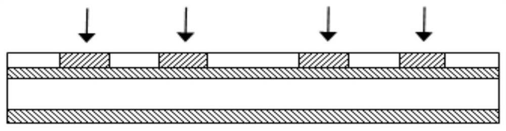
[0047] (1) Film: prepare the substrate 1 that has been roughened, degreased, cleaned and dried, such as Figure 1a As shown, a layer of dry film 2 is pasted on the upper and lower surfaces of the substrate, and after the dry film 2 is pasted, as shown in Figure 1b shown;

[0048] (2) Silver plating: such as Figure 1c Expose as shown, first align the black and white negative film with the substrate, and transfer the negative film pattern to the dry film 21 on the upper surface of the substrate; Figure 1d Develop as shown, remove the part of the dry film that has not undergone photopolymerization, and expose the local area 31 on the upper surface of the lead frame unit; since the lower surface needs to be electroplated with a nickel-palladium-gold layer, it does not need to be...

Embodiment 2

[0057] The pre-plating lead frame that embodiment one makes is used for square flat no-lead package (QFN), and processing technology comprises the steps:

[0058] First stick the ground wafer on the adhesive film, and then cut the wafer into individual separate chips along the dicing road;

[0059] Use silver glue to paste the chip on the chip seat of the lead frame unit, and connect the pins on the lead frame unit to the I / O port of the chip through welding wires to form a circuit connection;

[0060] Then use epoxy resin compound to wrap the chip, lead frame and bonding wire by injection molding to protect the function of the package component, and the nickel-palladium-gold plating layer on the lower surface of the lead frame unit is exposed for subsequent contact with the circuit board welding;

[0061] After molding, laser print on the surface of the package as a mark, and bake and cure in an oven at 175°C;

[0062] Finally, the unit is cut and separated from the non-fun...

Embodiment 3

[0064] Embodiment three provides a kind of pre-plating lead frame that is made by sticking film, silver-plating, nickel-palladium-gold, etching, removing film, and the preparation process is the same as embodiment one, and the only difference is that the silver plating solution in step (2) is low cyanide The high-speed silver plating solution has a pH value of 8.5 to 9.1, a silver concentration of 65 g / L, and a set current density of 20ASD; other parameters are the same as in Embodiment 1.

[0065] Sampling and measuring the thickness of the electroplated layer of the lead frame of the embodiment three by the method described in the embodiment one, the thickness of the silver-plated layer is in the range of 4.5~8.0 μm, the thickness of the nickel-plated layer is 0.5~1.5 μm, and the thickness of the palladium-plated layer is 0.05~ 0.15μm, and the thickness of the gold-plated layer is 0.005-0.015μm.

[0066] The roughness Ra of the upper surface of the lead frame prepared in Exa...


PUM

PropertyMeasurementUnit
Thicknessaaaaaaaaaa
Thicknessaaaaaaaaaa
Thicknessaaaaaaaaaa

Abstract

The invention belongs to the technical field of semiconductor devices, and particularly relates to a pre-electroplated lead frame and a preparation method thereof. The lead frame comprises a lead frame unit and a non-functional area, a silver plating layer is formed in a local area of the upper surface of the lead frame unit, a nickel-palladium-gold plating layer is formed in all exposed areas ofthe lower surface of the lead frame unit, and the side wall of the lead frame unit and the non-functional area on a frame body are free of electroplating layers. The lead frame is prepared through film pasting, silver plating, nickel-palladium-gold plating, etching and film stripping in sequence. According to the invention, a method of selective electroplating and etching in sequence is adopted, the upper surface is subjected to medium-low-speed, low-cyanide and low-temperature electroplating, and the obtained silver coating is high in compactness, uniform in thickness, smooth in surface and good in routing performance; the nickel-plated palladium-gold layer on the lower surface is resistant to high temperature and high humidity, has excellent storage time and good weldability, can providehigh air tightness and reliability for packaged products, and meets the production requirements of environmental protection and energy conservation.

Description

technical field [0001] The invention belongs to the technical field of semiconductor devices, and in particular relates to a pre-plating lead frame and a preparation method thereof. Background technique [0002] The lead frame is the basic component for the manufacture of integrated circuit semiconductor components. It provides a carrier for the chip of the integrated circuit, and realizes the connection of the chip and the electrical signal of the external circuit board by means of the bonding material. It can also provide a heat dissipation channel together with the package shell to release heat. Quad Flat No-leads (QFN) is the most common lead frame package structure. The traditional QFN process usually includes multiple steps such as chip bonding, chip cutting, chip welding, bonding, plastic molding, laser printing, electroplating, lead frame film bonding, and unit cutting. The process is complex, the production cycle is long, and the cost is high. Among them, the elect...

Claims


Application Information

Patent Timeline
IPC IPC(8): H01L23/495H01L21/48
CPCH01L21/4821H01L23/49548H01L23/49582
Inventor 黎超丰冯小龙林杰章新立林渊杰林海见罗壮
Owner NINGBO KANGQIANG ELECTRONICS CO LTD
Why Eureka
Try Eureka