Preparation method of electrochemical sensor electrode material for detecting aniline
A sensor electrode and electrochemical technology, applied in the direction of material electrochemical variables, gaseous chemical plating, metal material coating technology, etc., can solve the problems of complex coupling and synergistic effects, and achieve large detection range, high detection sensitivity, repeatability The detection effect is stable
- Summary
- Abstract
- Description
- Claims
- Application Information
AI Technical Summary
Problems solved by technology
Method used
Image

Examples
Embodiment 1
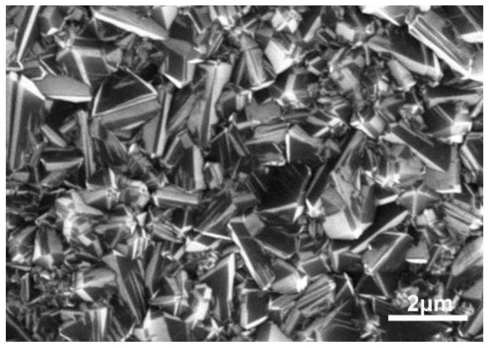
[0022] Embodiment 1: boron, nitrogen co-doped diamond film deposition
[0023] A p-type doped (100) single crystal silicon wafer was ground for 15 minutes with diamond powder with a particle size of 500 microns, and then placed in a microwave plasma chemical vapor deposition equipment chamber for boron and nitrogen co-doped diamond film deposition. During the deposition process, the microwave power was 1kW; the gas flow rate was 200 sccm hydrogen, 6 sccm methane, 2 sccm trimethyl borate, and 2 sccm nitrogen; the gas pressure was 8 kPa, the substrate temperature was 900 °C, and the growth time was 6 hours. Scanning electron microscope tests show that the boron and nitrogen co-doped diamond film grain structure obtained by growth is compact and complete, and the grain size is about 1 to 2 microns (see figure 1 ). Denoted as sample 1. The sample has good electrical conductivity, which meets the application requirements of electrochemical electrodes.
Embodiment 2
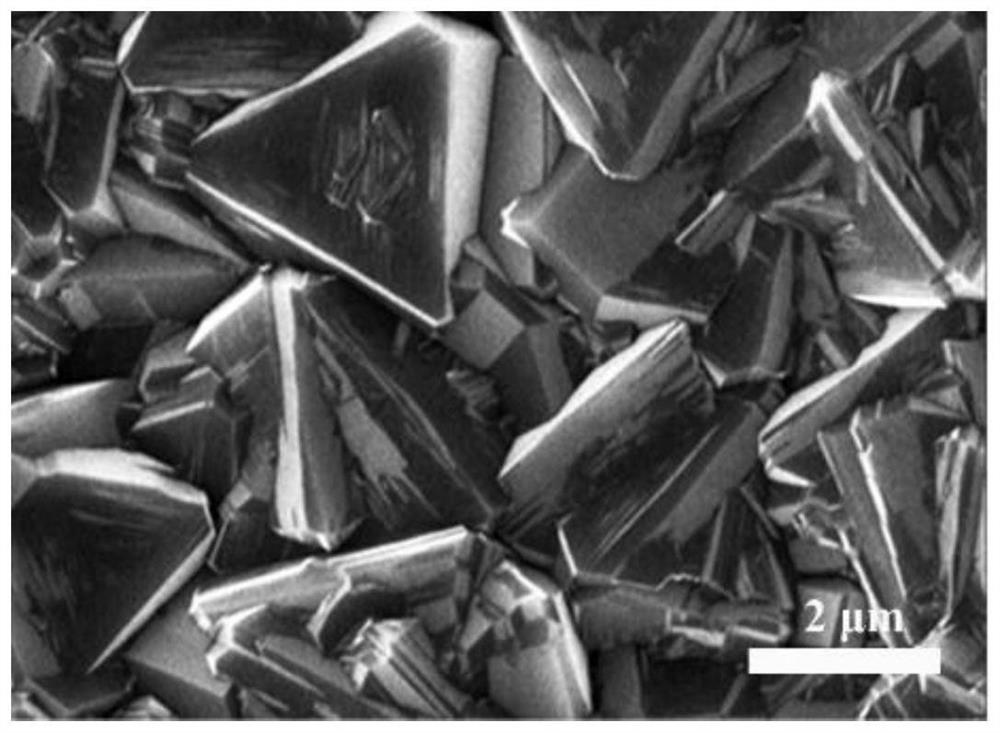
[0024] Embodiment 2: Boron-doped diamond film growth
[0025] A p-type doped (100) single crystal silicon wafer was ground for 15 minutes with diamond powder with a particle size of 500 microns, and then placed in a microwave plasma chemical vapor deposition equipment chamber for boron-doped diamond film deposition. The deposition gas flow rate is 200 sccm of hydrogen, 6 sccm of methane, and 2 sccm of trimethyl borate. The growth pressure was 8 kPa, the substrate temperature was 900° C., and the growth time was 6 hours. Scanning electron microscopy tests show that the grown boron-doped diamond film grain structure is compact and complete, and the grain size is about 2 to 3 microns (see figure 2 ). Denoted as sample 2. The sample has good conductivity, which meets the application requirements of electrochemical electrodes.
Embodiment 3
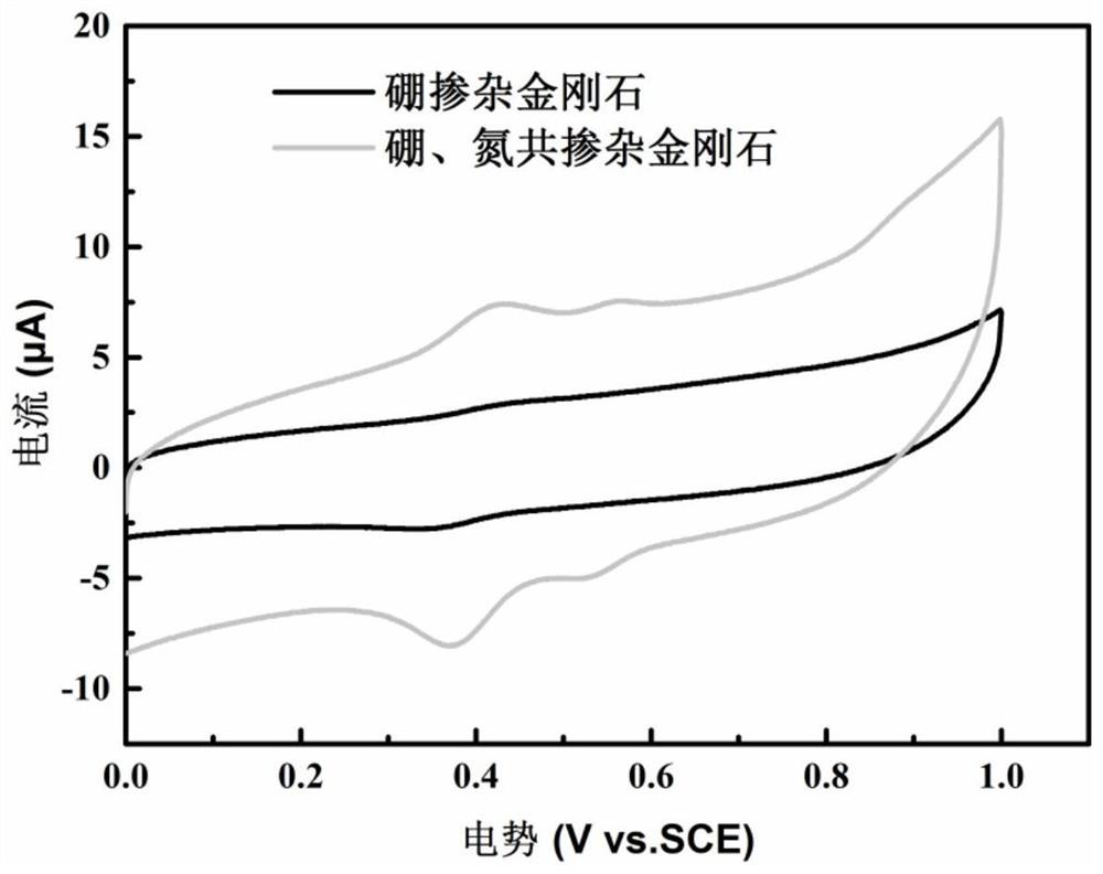
[0026] Example 3: Comparison of electrochemical properties of boron-doped and boron-nitrogen co-doped diamond films
[0027] The doped diamond films prepared in Example 1 and Example 2 were used to make electrochemical electrodes respectively, and the electrodes were tested by linear sweep voltammetry in 0.5M sulfuric acid solution. From the test results ( image 3 ) It can be seen that the potential window of the boron-nitrogen co-doped diamond electrode is almost as wide as that of the boron-doped diamond electrode, but its reaction current is much larger than that of the latter. The large reaction current makes the boron-nitrogen co-doped diamond electrode have higher test sensitivity than the boron-doped diamond electrode, so more excellent sensor performance can be obtained.
PUM
 Abstract
Description
Claims
Application Information
 - Generate Ideas
- Intellectual Property
- Life Sciences
- Materials
- Tech Scout
- Unparalleled Data Quality
- Higher Quality Content
- 60% Fewer Hallucinations
Browse by: Latest US Patents, China's latest patents, Technical Efficacy Thesaurus, Application Domain, Technology Topic, Popular Technical Reports.
© 2025 PatSnap. All rights reserved.Legal|Privacy policy|Modern Slavery Act Transparency Statement|Sitemap|About US| Contact US: help@patsnap.com