Homoepitaxial gallium nitride high-electron-mobility transistor based on P-type GaN electric leakage isolation layer and manufacturing method of homoepitaxial gallium nitride high-electron-mobility transistor

A technology with high electron mobility and gallium nitride, applied in the field of high electron mobility transistors, can solve the problem of reducing the breakdown voltage and output power density of the device, increasing the difficulty of the material growth process and parasitic pollution, and affecting the output of the device current and power. characteristics and other issues, to achieve the effect of improving breakdown voltage and working reliability, increasing process repeatability and consistency, and reducing high-ohmic contact resistance

Active Publication Date: 2021-10-26
XIDIAN UNIV
View PDF6 Cites 0 Cited by
  • Summary
  • Abstract
  • Description
  • Claims
  • Application Information

AI Technical Summary

Problems solved by technology

[0004] First, heteroepitaxial gallium nitride materials need to adopt a nucleation layer structure. The growth process, structure and thickness of the structure directly determine the crystallization quality and transport characteristics of the heterostructure material on it, and the process control is difficult and repeatable. and poor consistency
[0005] The second is that the heterogeneous epitaxial GaN material has high-density dislocation defects, which cause the device to form a leakage channel under the condition of long-term high-voltage bias operation, reduce the breakdown voltage of the device, and trap electrons at the same time, causing the current collapse of the device and reliability degradation
[0006] The third is that there is a high concentration of n-type Si impurities at the homoepitaxial interface during the homoepitaxial GaN material. This impurity will be introduced into the bulk leakage channel and it is difficult to completely remove it, which seriously reduces the breakdown voltage and output power density of the device.
[0007] Fourth, when metal-organic chemical vapor deposition technology is used to homoepitaxially epitaxial GaN materials, iron doping or carbon doping is required to compensate for the high concentration of Si impurities at the homoepitaxial interface, which increases the difficulty of material growth process and parasitic pollution.
[0008] The fifth is to make the source-drain electrodes directly on the surface of the barrier layer. The ohmic contact resistance of the source-drain electrodes is high, which affects the output characteristics of the device such as current and power.

Method used


Image

  • Homoepitaxial gallium nitride high-electron-mobility transistor based on P-type GaN electric leakage isolation layer and manufacturing method of homoepitaxial gallium nitride high-electron-mobility transistor
  • Homoepitaxial gallium nitride high-electron-mobility transistor based on P-type GaN electric leakage isolation layer and manufacturing method of homoepitaxial gallium nitride high-electron-mobility transistor
  • Homoepitaxial gallium nitride high-electron-mobility transistor based on P-type GaN electric leakage isolation layer and manufacturing method of homoepitaxial gallium nitride high-electron-mobility transistor

Examples


Embodiment 1

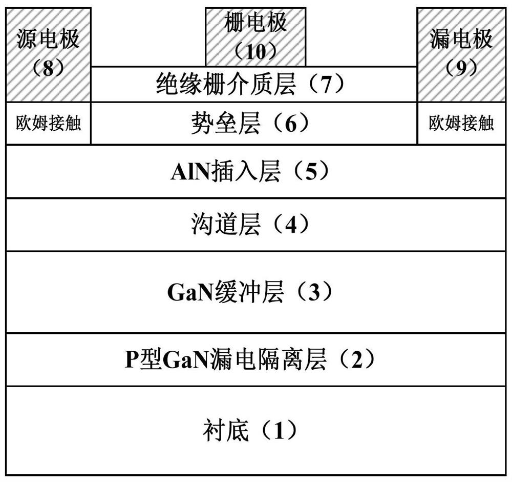
[0048]Embodiment 1, a homoepitaxial gallium nitride high electron mobility transistor with a self-supporting gallium nitride substrate, a GaN channel layer with a thickness of 20 nm, and an AlGaN barrier layer with a thickness of 30 nm is used as the fabrication substrate.

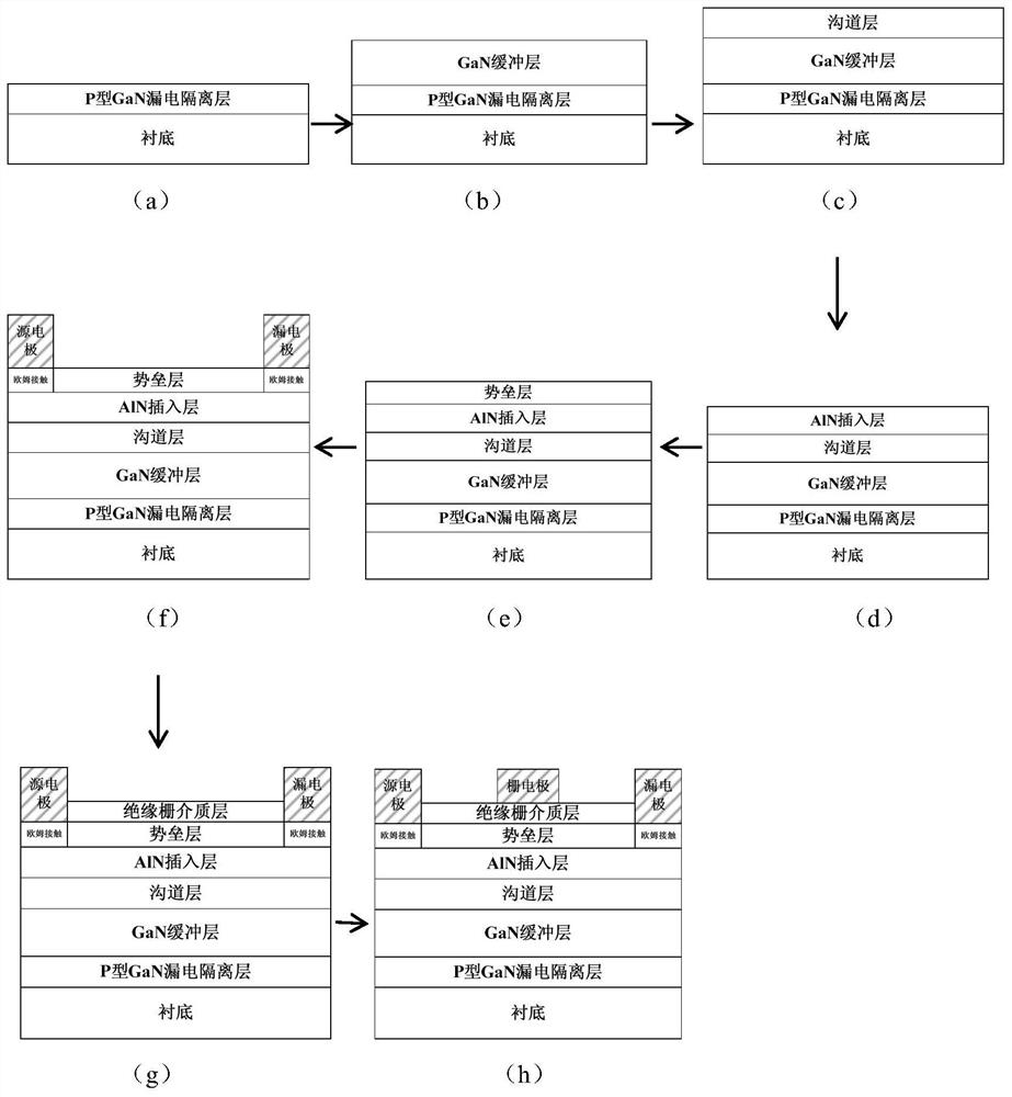
[0049] Step 1, depositing a P-type GaN leakage isolation layer, such as image 3 (a).

[0050] A self-supporting gallium nitride substrate is selected and placed in a reaction chamber, and a P-type GaN leakage isolation layer with a thickness of 500nm is deposited by metal-organic chemical vapor deposition technology.

[0051] The process conditions used to deposit the P-type GaN leakage isolation layer are: temperature 1100°C, pressure 40Torr, ammonia gas flow rate 2000 sccm, gallium source flow rate 100 sccm, magnesium source flow rate 20 sccm, nitrogen gas flow rate 3000 sccm.

[0052] Step 2, depositing a GaN buffer layer, such as image 3 (b).

[0053] A GaN buffer layer with a thickness of 10 μm i...

Embodiment 2

[0071] In the second embodiment, a homoepitaxial gallium nitride high electron mobility transistor with a thick-film gallium nitride substrate material, an InGaN channel layer with a thickness of 10 nm, and an InAlN barrier layer with a thickness of 12 nm is used as the fabrication substrate.

[0072] Step 1, depositing a P-type GaN leakage isolation layer on the thick-film gallium nitride substrate material, such as image 3 (a).

[0073] Select the thick-film GaN substrate material and place it in the reaction chamber, using metal organic chemical vapor deposition technology, at a temperature of 1050 ° C, a pressure of 40 Torr, an ammonia gas flow of 2000 sccm, a gallium source flow of 120 sccm, nitrogen A P-type GaN leakage isolation layer with a thickness of 100nm is deposited on the thick-film gallium nitride substrate material under the process conditions that the flow rate is 3000sccm and the flow rate of the magnesium source is 30sccm.

[0074] Step 2, depositing a Ga...

Embodiment 3

[0087] Embodiment 3, a homoepitaxial gallium nitride high electron mobility transistor with a self-supporting gallium nitride substrate, a GaN channel layer thickness of 50 nm, and a ScAlN barrier layer thickness of 5 nm is used as the fabrication substrate.

[0088] Step A, select a self-supporting gallium nitride substrate, and place it in a reaction chamber, using metal-organic chemical vapor deposition technology, at a temperature of 1150 ° C, a pressure of 40 Torr, an ammonia flow rate of 2000 sccm, and a gallium source flow rate of 90sccm, the flow rate of nitrogen gas is 3000sccm, and the flow rate of magnesium source is 10sccm, a P-type GaN leakage isolation layer with a thickness of 1000nm is deposited on the free-standing gallium nitride substrate, as image 3 (a).

[0089]Step B, using metal-organic chemical vapor deposition technology, under the process conditions of temperature 1150°C, pressure 40 Torr, ammonia gas flow rate 2000 sccm, gallium source flow rate 90 ...


PUM

PropertyMeasurementUnit
thicknessaaaaaaaaaa
thicknessaaaaaaaaaa
thicknessaaaaaaaaaa

Abstract

The invention discloses a homoepitaxial gallium nitride high-electron-mobility transistor based on a P-type GaN electric leakage isolation layer and a manufacturing method of the homoepitaxial gallium nitride high-electron-mobility transistor. The transistor comprises a substrate, a channel layer, an AlN insertion layer and a barrier layer from bottom to top, the substrate is made of a self-supporting gallium nitride substrate or a thick-film gallium nitride substrate material, and a P-type GaN electric leakage isolation layer and a GaN buffer layer are arranged between the substrate and the channel layer and used for isolating and shielding a parasitic electric leakage channel caused by Si impurity adsorption on the surface of the substrate; an insulated gate dielectric layer and a gate electrode are sequentially arranged on the upper portion of the barrier layer, ohmic contact areas are arranged on the two sides of the barrier layer respectively, and a source electrode and a drain electrode are arranged on the ohmic contact areas respectively. The dislocation density of the heteroepitaxial gallium nitride material can be effectively reduced, parasitic electric leakage of a homoepitaxial interface of the gallium nitride material is isolated, the control difficulty of a material epitaxial process is reduced, the breakdown voltage, the output power and the working reliability of a device are improved, and the method can be applied to microwave power amplifiers and radio frequency integrated circuit chips.

Description

technical field [0001] The invention belongs to the technical field of semiconductor devices, and in particular relates to a high electron mobility transistor, which can be used for making solid-state microwave power amplifiers and radio frequency integrated circuit chips. Background technique [0002] High electron mobility transistors based on wide-bandgap nitride semiconductor materials have the advantages of high frequency, high power, high efficiency, and high temperature resistance, and are the main devices for preparing solid-state microwave power amplifiers. After more than 20 years of experimental research, the performance and reliability of the device have been improved, and it has gradually entered the field of commercial application from experimental research, and has been widely used in electronic equipment such as 5G communication and information detection. In order to further improve the operating frequency, output power and efficiency of GaN HEMT devices, it ...

Claims


Application Information

Patent Timeline
Patent Type & Authority Applications(China)
IPC IPC(8): H01L29/778H01L21/335H01L29/45H01L29/20H01L29/06
CPCH01L29/778H01L29/66462H01L29/452H01L29/2003H01L29/0611
Inventor 薛军帅李祖懋吴冠霖郝跃张进成杨雪妍张赫朋姚佳佳孙志鹏刘芳
Owner XIDIAN UNIV
Why Eureka
Try Eureka