
Quanta dot active region structure of broad spectrum white light LED and epitaxial growth method thereof

A quantum dot active region, epitaxial growth technology, applied in electrical components, circuits, semiconductor devices, etc., can solve problems such as poor white light color rendering index, high device operating voltage, and no LED materials and devices involved

Inactive Publication Date: 2005-03-16
TSINGHUA UNIV
View PDF0 Cites 30 Cited by
  • Summary
  • Abstract
  • Description
  • Claims
  • Application Information

AI Technical Summary

Problems solved by technology

[0013] 2. GaN-LEDs of two colors (different In compositions) by direct epitaxy (reference J.Han and A.V.Nurmikko, IEEE, Jour.of Sel.Top.Quan.Elect., Vol.8(2002), No. 2, pp.289-297), that is, the main epitaxy sequence from the substrate up is: buffer layer-n-type layer (1)-active region (1)-p-type region (1)-tunneling layer-n-type Layer (2)-active region (2)-p-type region (2), using a two-step dry etching process to obtain the etching mesa of n-type layer (1) and n-type layer (2), respectively, After applying forward working voltage to the contact layer of p-type region (2), applying reverse working voltage to the table top of n-type layer (1), and grounding (0V) on the table top of n-type layer (2), two colors can be turned on at the same time The LED emits white light. In this way, it is a three-terminal device, and the manufacturing steps are complicated;
[0014] 3. GaN-LEDs of two colors (different In compositions) by direct epitaxy (reference C.H.Chen, S.J.Chang, Y.K.Su, et al, IEEE, Photo.Tech.Lett., Vol.14(2002), No. 7, pp.908-910 and literature C.H.Chen, S.J.Chang, Y.K.Su, Phys.Stat.Sol.(c), Vol.0(2003), No.7, pp.2257-2260): buffer layer-n Type layer (1)-active area (1)-p-type area (1)-n-type gradient layer-n-type layer (2)-active area (2)-p-type area (2), but only etching After the n-type layer (1) mesa is exposed, a forward working voltage is applied to the contact layer of the p-type region (2), and after the n-type layer (1) mesa is grounded (0V), cascade light is emitted. The device works in this way higher voltage;
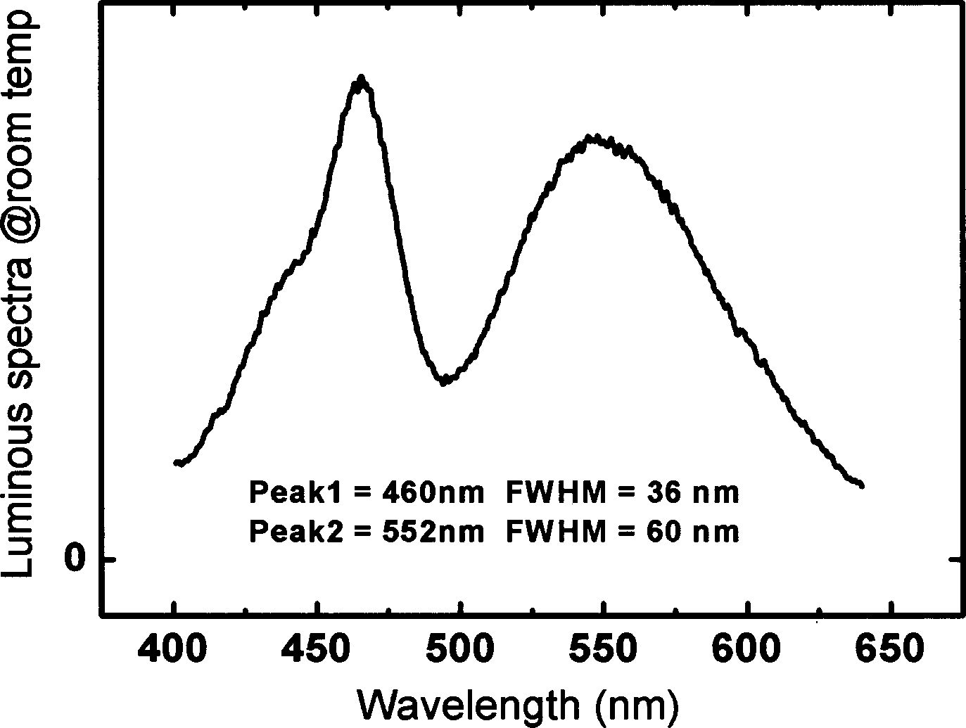
[0015] 4. InGaN quantum well active region with high In composition (In% can be as high as 70%) (references C.H.Chen, S.J.Chang, Y.K.Su, Jpn.J.Appl.Phys., Vol.42 (2003), Part 1, No.4B, pp.2281-2283), when the injection current of the LED device increases from 1mA to 150mA, the emitted spectrum shifts greatly, and the human visual perception is: orange (orange)- Yellow (yellow)-yellowish green (yellowish green)-yellowish white (yellowish white), the color rendering index of white light obtained in this way is poor;
[0016] 5. Si and Zn co-doping technology using InGaN active region (references J.K.Sheu, C.J.Pan, G.C.Chi, etal, IEEE, Photo.Tech.Lett., Vol.14(2002), No.4, pp .450-452), in its luminescence spectrum, there are both short-wavelength side active region quantum well near-band-edge emission components and long-wavelength side donor-acceptor pair luminescent recombination broad-spectrum components, thereby obtaining white light Effect, this method belongs to impurity luminescence and low efficiency
[0022] References Y.G.Kim, Y.S.Joh, J.H.Song, K.S.Baek, S.K.Chang, and E.D.Sim Appl.Phys.Lett.Vol.83, 2656 (2003), literature F.Tinjod, B.Gilles, S.Moehl, K. Kheng, and H.Mariette Appl.Phys.Lett.Vol.82, 4340 (2003) and literature H.S.Lee, K.H.Lee, J.C.Choi, H.L.Park, T.W.Kim, and D.C.Choo Appl.Phys.Lett.81, 3750 (2002 ) The research work on II / VI compound semiconductor quantum dots is mainly to evaluate and study the optical and electrical properties of the quantum dot active region, and none of them involve the use of quantum dot active regions to produce direct white light without using fluorescence Converted LED Materials and Devices

Method used


Image

  • Quanta dot active region structure of broad spectrum white light LED and epitaxial growth method thereof
  • Quanta dot active region structure of broad spectrum white light LED and epitaxial growth method thereof
  • Quanta dot active region structure of broad spectrum white light LED and epitaxial growth method thereof

Examples


Embodiment 1

[0075] The MOCVD epitaxial growth of LED materials containing a single type of indium gallium nitride / gallium nitride (InGaN / GaN) quantum dot buried structure in the active area is carried out to achieve wide-spectrum white light. Its extension sequence is as Figure 4 Shown: sapphire substrate 1, GaN buffer layer 2 (thickness about 80nm-100nm), n-type GaN bulk material and ohmic contact layer 3 (thickness about 4000nm), n-type AlGaN barrier layer and GaN isolation layer 4 (thickness About 50nm), InGaN quantum dot active region 5 (thickness 20nm-70nm), GaN isolation layer and p-type AlGaN barrier layer 6 (thickness about 40nm), p-type GaN ohmic contact layer 7 (thickness 150nm-250nm).

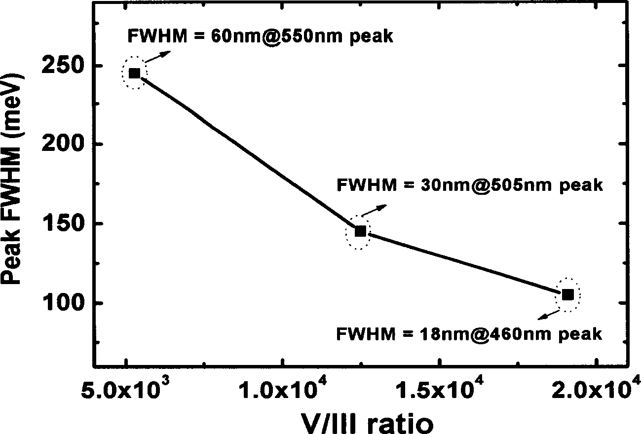
[0076] Among them: the Al% of the n-type and p-type AlGaN barrier layers is 8%-12%; the average In composition of the quantum dot active area and the quantum dot nucleation / agglomeration rate are jointly controlled by TEGa, TMIn flow rate and substrate temperature. When TEGa flow rate is 87sccm (10...

Embodiment 2

[0078] Perform MOCVD epitaxial growth of LED materials containing a single type of indium gallium nitride / indium gallium nitride (InGaN / InGaN) quantum dot buried structure in the active area to achieve wide-spectrum white light. Its extension sequence is as Figure 6 Shown: sapphire substrate 1, GaN buffer layer 2 (thickness about 80nm-100nm), n-type GaN bulk material and ohmic contact layer 3 (thickness about 4000nm), n-type AlGaN barrier layer and GaN isolation layer 4 (thickness About 50nm), InGaN barrier region 5 (In%-10%, thickness 10nm-15nm), InGaN quantum dot active region 6 (thickness about 20nm~70nm), GaN barrier region and isolation layer 7 (thickness about 10nm-15nm) ), a p-type AlGaN barrier layer 8 (with a thickness of about 40 nm), and a p-type GaN ohmic contact layer 9 (with a thickness of 150 nm to 250 nm).

[0079] Among them: the Al% of the n-type and p-type AlGaN barrier layers is 8%-12%; the average In composition of the quantum dot active area and the quantum ...

Embodiment 3

[0081] Conduct MOCVD epitaxial growth of LED materials with multiple types of indium gallium nitride / gallium nitride (InGaN / GaN) quantum dot buried structures and indium gallium nitride / gallium nitride (InGaN / GaN) quantum well layers cascaded in the active area, Achieve wide-spectrum white light. Its extension sequence is as Figure 8 Shown: sapphire substrate 1, GaN buffer layer 2 (thickness about 80nm-100nm), n-type GaN bulk material and ohmic contact layer 3 (thickness about 4000nm), n-type AlGaN barrier layer and GaN isolation layer 4 (thickness About 50nm), InGaN / GaN multiple quantum well active region 5 (repetition period is 3, InGaN quantum well thickness is about 2nm, GaN barrier region thickness is about 10nm), InGaN quantum dot light emitting region 6 (thickness is about 20nm~70nm), GaN isolation layer 7 (thickness of about 10 nm-15 nm), p-type AlGaN barrier layer 8 (thickness of about 40 nm), p-type GaN ohmic contact layer 9 (thickness of 150 nm to 250 nm).

[0082] Amon...


PUM


Abstract

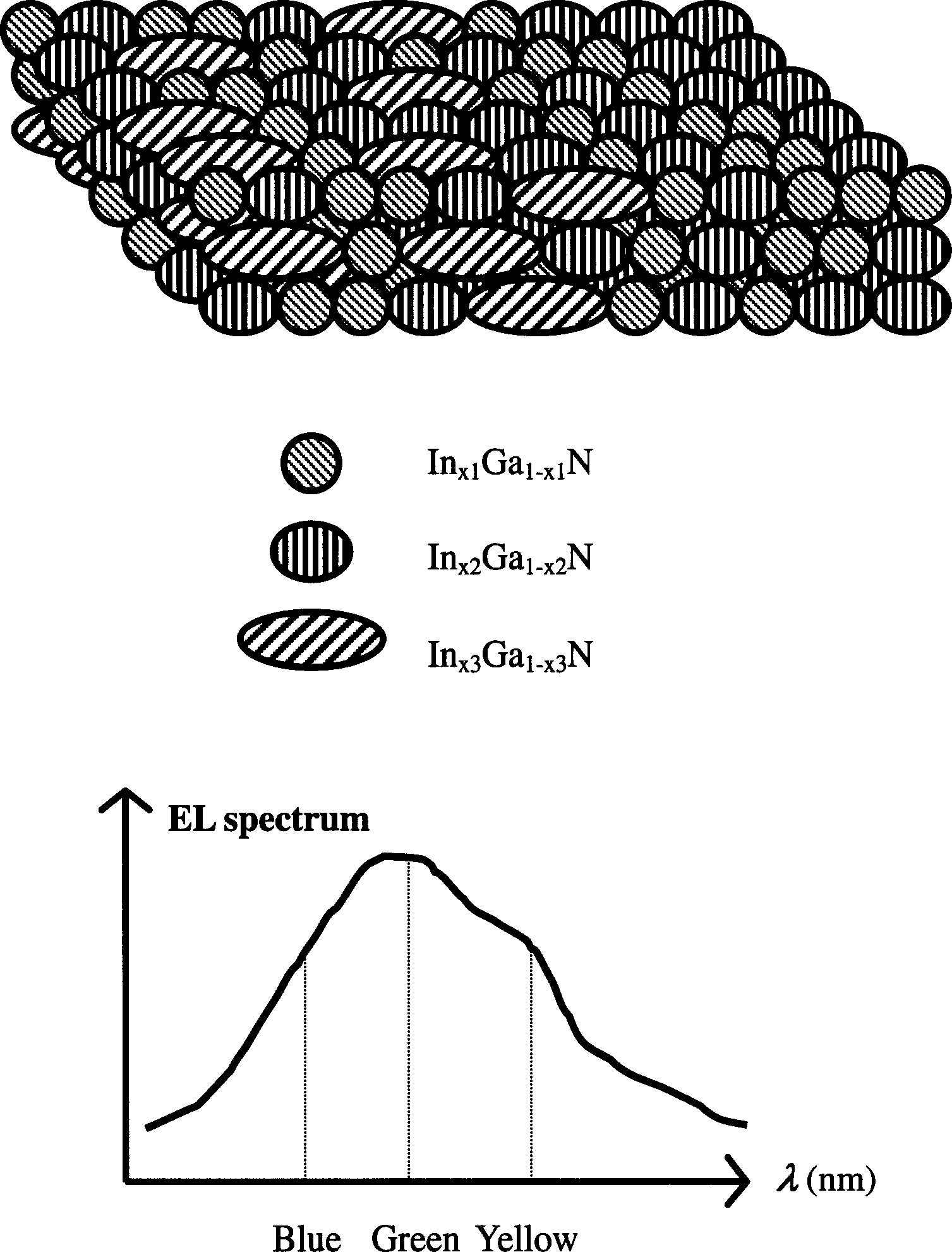
The invention relates to a quantum point active area structure of wide spectral white light LED and its growing method, based semiconductor power-typed light emitting diode of gallium nitride III / V group compounds, metal organic chemistry gas sediment growing method and relative active area structure design of white light power-typed spectral light emitting diode LED material with use solid state light source whose active area contains indium-gallium-nitrogen- gallium-nitrogen or quantum point of indium-gallium-nitrogen- gallium-nitrogen structure. It supplies several kinds of new machinery structure design based on InGaN quantum point active area, and core growth parameter of condition for extension such as flux of reaction source, V / III ratio and temperature of substrate. The invention can realize transformation without fluorescence, high color-rendering index and luminance requirement of highly luminous GaN white light LED, also, it is suitable for(CdSe) ZnS / ZnSe, (Zn, Cd)Se / ZnSe, (Zn, Cd, Hg)(Se,Te) / ZnSe, (Zn,Cd,Hg)(Se,Te) / ZnS and other II / VI group compounds semiconductor containing quantum point of spectral power-typed light emitting diode material growing, whose main light emitting diode is them same with that of III / V InGaN group quantum point 21 .

Description

Technical field [0001] The invention relates to an active area containing indium gallium nitride (GaN) III / V compound semiconductor power light emitting diode (Light Emitting Diode, LED) based on gallium nitride (GaN) and applied to a novel all-solid-state lighting source. Metal-Organic Chemical Vapor Deposition (Metal-Organic-) of white light power wide-spectrum light-emitting diode LED materials with gallium-nitrogen (InGaN / GaN) or indium-gallium-nitrogen-indium-gallium-nitride (InGaN / InGaN) quantum dots (Quantum Dots, QDs) structure Chemical-Vapour-Deposition, MOCVD; or Metal-Organic-Vapour-Phase-Epitaxy, MOVPE) epitaxial growth technology and related active area structure design. At the same time, the technology of the present invention is also applicable to II / VI group compound semiconductors such as (zinc / cadmium / mercury) / (sulfur / selenium / tellurium) ((CdSe)ZnS / ZnSe, (Zn,Cd)Se / ZnSe, (Zn, Cd, Hg) (Se, Te) / ZnSe, (Zn, Cd, Hg) (Se, Te) / ZnS), epitaxial growth and device fabricatio...

Claims


Application Information

Patent Timeline
Patent Type & Authority Applications(China)
IPC IPC(8): H01L33/00H01L33/04
Inventor 罗毅邵嘉平韩彦军孙长征郝智彪
Owner TSINGHUA UNIV
Learn More