Vertical type wide bandgap semiconductor device structure and making method

A wide-bandgap semiconductor and device structure technology, applied in the field of microelectronics, can solve problems such as the inability to meet the needs of high-power device development, and achieve the effects of reducing defect density and lattice mismatch.

Inactive Publication Date: 2006-02-08
XIDIAN UNIV
View PDF0 Cites 7 Cited by
  • Summary
  • Abstract
  • Description
  • Claims
  • Application Information

AI Technical Summary

Problems solved by technology

Although this solution improves the heat dissipation capability of the device to a certain extent, due to the inherent limitations of the planar process and the continuous improvement of the power density and integration of the device, this solution has been unable to meet the needs of further development of high-power devices.

Method used


Image

  • Vertical type wide bandgap semiconductor device structure and making method
  • Vertical type wide bandgap semiconductor device structure and making method
  • Vertical type wide bandgap semiconductor device structure and making method

Examples


example 1

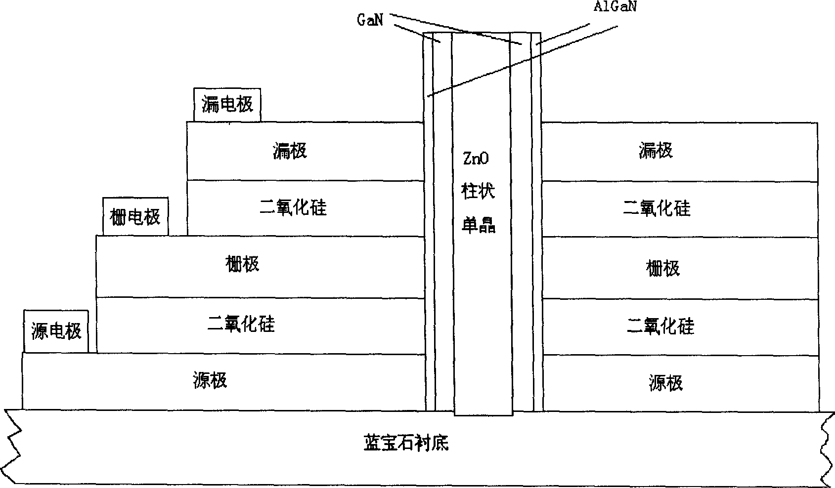
[0039] The invention manufactures a vertical single tube AlGaN / GaN HFET device based on ZnO nano columnar single crystal.

[0040] Epitaxial layer material selection: AlGaN, GaN.

[0041] Vertical single crystal material selection: ZnO.

[0042] Substrate material selection: (2-1-10) crystal plane of single crystal sapphire.

[0043] Metal material selection: Au, Ti / Ag, Al.

[0044] Dielectric material selection: SiO 2 .

[0045] Refer to image 3 , The structure and manufacturing process of the device in this example are as follows:

[0046] 1. Growth of ZnO nano columnar single crystal

[0047] The first step is the fabrication of a single-layer self-assembled submicron ball array.

[0048] Choose sapphire as the substrate. The colloidal crystal method is used to make the sub-micron sphere array, and the selected colloidal crystal is polystyrene sub-micron spheres, and the diameter of the polystyrene spheres is about 895 nm. Firstly, ultrasonically degrade the substrate for 20 m...

example 2

[0070] The invention manufactures a vertical single-tube AlGaN / GaN HFET device based on a ZnO nano-belt single crystal.

[0071] Epitaxial layer material selection: AlGaN, GaN.

[0072] Vertical single crystal material selection: ZnO.

[0073] Substrate material selection: polycrystalline sapphire.

[0074] Metal material selection: Au, Ti / Ag, Al.

[0075] Dielectric material selection: Si 3 N 4 .

[0076] Refer to Figure 4 , The structure and manufacturing process of the device in this example are as follows:

[0077] 1. Growth of ZnO nano-ribbon single crystal

[0078] In this example, the ZnO nano-ribbon single crystal is grown by the VS mechanism, and the selected substrate is a sapphire polycrystalline material. The raw materials used are ZnO powder and 1% Li 2 O powder. First, the raw materials are mixed and placed on the alumina boat in the center of the alumina test tube, and the sapphire polycrystalline substrate material is placed at the downstream position of the alumi...

example 3

[0096] The invention manufactures an air-isolated vertical mesh AlGaN / GaN microwave power device based on an array of ZnO nano-columnar single crystals.

[0097] Epitaxial layer material selection: AlGaN, GaN

[0098] Vertical single crystal material selection: ZnO

[0099] Substrate material selection: n-type doped GaN conductive material;

[0100] Selection of metal materials: Au, Ti / Ag, Al

[0101] Medium material selection: air

[0102] Refer to Figure 5 , The structure and production process of this example are as follows:

[0103] 1. Growth of arrayed ZnO nano columnar single crystals

[0104] The first step is to make a catalyst template

[0105] First, deposit a thin layer of Au catalyst on the GaN substrate by thermal evaporation;

[0106] Then, according to the distribution density of the devices and heat dissipation requirements, design and manufacture the photolithography mask;

[0107] Finally, a layer of photoresist is covered on the surface of the Au catalyst layer,...


PUM


Abstract

The invention discloses a vertical semiconductor component structure and preparing method, f or resolving the high defect concentration of wide forbidden band semiconductor materials / components and the heat dissipation of high power devices. The inventive structure exploits three-dimensional nanometer structure and comprises: substrate, vertical single crystal, epitaxial layer, metal layer, medium layer, wherein the vertical single crystal is vertical to the substrate, the epitaxial layer is vertical to the vertical single crystal and the metal layer is parallel to the surface of the substrate, and at least one layer, the medium layer is parallel between each metal layers for isolation; the surface of metal layer and epitaxial layer form the ohmic contact or rectifying contact; connecting out leads on the surface of metal layers. The invention has the advantages of good dissipation of heat, high electric property.

Description

Technical field [0001] The invention belongs to the field of microelectronics technology, and relates to semiconductor materials and device manufacturing technology. Specifically, it is a structure of a semiconductor device and a manufacturing method thereof, which can be used to manufacture high-quality heterostructure devices, high-power devices, etc., and can be effective Reduce the defect density of the material and improve the heat dissipation performance of the device. Background technique [0002] In recent years, because the third-generation wide-bandgap semiconductors represented by silicon carbide SiC and gallium nitride GaN have large forbidden band width, high critical field strength, high thermal conductivity, high carrier saturation rate, and two-dimensional heterojunction interface The high concentration of electron gas and other excellent characteristics have attracted widespread attention. In theory, the high electron mobility transistor HEMT, heterojunction bipo...

Claims


Application Information

Patent Timeline
Patent Type & Authority Applications(China)
IPC IPC(8): H01L29/78H01L21/336
Inventor 郝跃王中林陈军峰张进城张春福
Owner XIDIAN UNIV
Why Eureka
Try Eureka