Dielectric ink composition

a technology of dielectric ink and composition, applied in the direction of dielectric characteristics, inks, printing, etc., can solve the problems of poor interconnection performance and reliability, system incompatibility with conductive layers, and inability to stretch, so as to improve thermal and reliability properties of devices, reduce the effect of resistivity change and high resistivity

Active Publication Date: 2021-12-07
FRY S METALS INC
View PDF18 Cites 0 Cited by
  • Summary
  • Abstract
  • Description
  • Claims
  • Application Information

AI Technical Summary

Benefits of technology

[0025]It is an object of the present invention to provide a composite dielectric powder or flake that is capable of producing a dielectric ink composition which is high in resistivity, exhibits minimal change in resistivity after a thermal shock test, is capable of passing a humidity and DC applied test, and is capable of improving thermal and reliability properties of devices.
[0026]It is another object of the present invention to provide a dielectric ink composition for forming electric circuits which are highly flexible and that can be printed on a substrate that undergoes stretching or bending with 10% strain without sacrificing physical properties of the dielectric material.
[0027]It is still another object of the present invention to provide a dielectric ink composition for forming electronic circuits that is high in resistivity, capable of improving the probability of contact between the dielectric material, increasing insulating properties of the electric circuits, and that exhibits excellent migration resistance.

Problems solved by technology

However, the composition is not stretchable, and the presence of water makes the system incompatible with the conductive layer.
However, these inorganic devices undergo a significant change under stretching, leading to poor interconnect performance and reliability.
However, the hardening agent is flaky and hard, and it is not applicable to manufacturing flexible circuits.
However, the dielectric ink is prone to forming a gel after being kept in storage for an extended time.
The ability to create a complex thermoformed in-mould device comprising multiple layers of graphic inks, conductive circuitry, insulating layers, as well as various electronic elements such as displays, lighting, sensors, and the like, has been difficult to achieve in practice.
In addition, many such inks are effectively incompatible with each other, with the various printed layers insufficiently adhering to each other, resulting in an unstable electrical or electronic device.
For example, an insulating (dielectric) ink which is printed over a conductive ink may leave gaps or subsequently shear or peel away, resulting in inadequate insulation in the resulting electrical, electronic or optoelectronic device.
Known UV-curable inks are not appropriate for use in functional electronic devices constructed entirely using printing technology.
The few that are designed for this type of application either do not have the optical clarity required for fully printed optoelectronics devices or can only be overcoated or overprinted with another UV curable ink, not a heat curable ink.
Finally, it is not believed that any of the known inks have the ability to withstand severe forming.
UV curable compositions are generally not suitable for heat treatment.
In some instances, a thermoformed system of a layered dielectric over a printed conductive circuit undergoes severe cracking due to the incompatibility of the dielectric layer with the printed electronic circuit or due to the inability of the printed circuit to deform without cracking during the thermoforming process.
Another difficulty is maintaining resistance in a printed circuit which contains a binder system that also allows for deformation without cracking.
In many instances, the binder system acts as an insulator for the conductive dispersed phase to such a degree that although the circuit can be formed without cracking, it does not have sufficient conductivity to function reliably in a printed and thermoformed device.
Known dielectric inks are also generally not suitable for selective structuring and stretching in the UV range, as required, for example, in in-mould applications and for printed dielectrics in microelectronics.
Also, known dielectric inks do not exhibit the required continuity to environmental characteristics which are required for specific applications such as forming.
In conventional dielectric ink compositions, common resins, such as epoxy resins, are flaky and hard, which is of limited use in making stretchable interconnects.
Other polymeric inks have the disadvantage of non-flexibility.
As a result, the functional circuit made of the dielectric ink is prone to cracking.
It is a technical challenge to simultaneously achieve the requirements of electric performance, such as high resistance, thermal stability, good adhesion to conductive layer, processing performance and desired level of bending and forming characteristics.
Micro-electronic circuits are typically made using expensive deposition, plating and etching technologies.
Such technologies typically require significant investments, and clean MOM atmospheres.
It is often time consuming and expensive to make slight variations in components, accordingly, manufacturing lines are often set up for a single application.
Accurate placement and formation of the dielectric layers using conventional techniques is often time consuming and requires specialized equipment.

Method used


Image

  • Dielectric ink composition
  • Dielectric ink composition
  • Dielectric ink composition

Examples


example 1

Curable Dielectric Ink

[0118]An organic medium for the composition of the invention was prepared as follows: 15 grams of a linear aromatic polyester resin (Dynapol, available from Evonik) was added to 170 grams of magnetically stirred carbitol acetate (boiling point 230° C.) and 40 g Dowanol EPh glycol ether (available from Dow Chemicals). A rheology modifier, resin and adhesion promoter were also added to the mixture. The mixture was heated to 60° C. and stirred at this temperature until a clear solution was achieved (approximately 4 hours). The solution was allowed to cool slowly to ambient temperature.

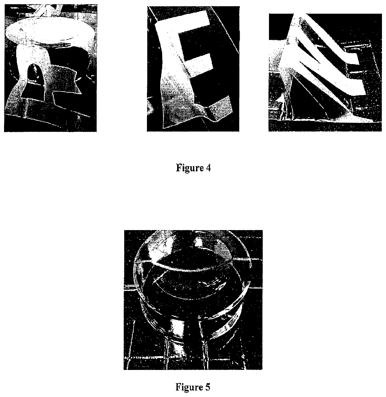
[0119]The viscosity of the resulting dielectric ink composition after 24-hour ambient temperature rest was measured at about 12,000 centipoise (at 20° C.) on a Brookfield RVT viscometer, 5 rpm, No. 5 spindle. The dielectric ink composition was printed on a 100-micron thick electrical grade PET film through a 0.50 mil silk screen. The printed parts were dried in a laboratory air circu...

example 2

[0127]A dielectric ink was obtained by the same procedure described in Example 1 except that 250 parts by weight (25% by weight) of a talc powder with predominant particle size in the range from about one to about twenty microns, an average major particle diameter of 2 μm was blended and dispersed uniformly by a mixing and grinding machine and to obtain stretchable and formable dielectric ink. This composition also contained a polyester polyol.

example 3

[0128]A dielectric ink was obtained by the same procedure described in Example 1, except that the composition used no solvents.


PUM

PropertyMeasurementUnit
boiling pointaaaaaaaaaa
temperatureaaaaaaaaaa

Abstract

The present invention relates to flexible and stretchable UV and thermally curable dielectric ink compositions that can be thermo or vacuum formed. The flexible ink can form a stretchable dielectric coating having excellent adhesion. The dielectric ink compositions can be applied on a circuit board, such as a paper-phenolic resin board, plastic board (PMMA, PET or the like) or a glass-epoxy resin board, by screen printing or the like, followed by heat / UV curing. The compositions are suitable for use in applications such as a capacitive touch, in-mold forming, creating cross over insulation layers, and manufacturing electronic circuitry and devices.

Description

CROSS-REFERENCE TO RELATED APPLICATIONS[0001]The present application claims the benefit of U.S. provisional application Ser. No. 62 / 506,095, filed in May 15, 2017, the subject matter of which is herein incorporated by reference in its entirety.FIELD OF THE INVENTION[0002]The invention relates to screen-printable and dispensable dielectric ink compositions for stretchable electronic surfaces.BACKGROUND OF THE INVENTION[0003]A dielectric material (otherwise known as a “dielectric”) is an electrical insulator that is capable of being polarized by an applied electric field. Examples include, but are not limited to, porcelain (ceramic), mica, glass, plastics, and the oxides of various metals. Dry air is also an excellent dielectric and is used in variable capacitors and some types of transmission lines. Distilled water is a fair dielectric. A vacuum is an exceptionally efficient dielectric.[0004]An important property of a dielectric is its ability to support an electrostatic field white ...

Claims


Application Information

Patent Timeline
Patent Type & Authority Patents(United States)
IPC IPC(8): C09D11/322B41F15/40B41M5/00C09D11/037C09D11/101C09D11/102C09D11/104C09D11/107C09D11/38H05K1/03H05K3/00C09D11/30
CPCC09D11/322B41F15/40B41M5/0023C09D11/037C09D11/101C09D11/102C09D11/104C09D11/107C09D11/38H05K1/0393H05K3/0011C09D11/30H05K2201/0133C09D11/10C09D11/52
Inventor PUJARI, NARAHARISUNDARAMURTHY, JAYAPRAKASHSARKAR, SIULIBHATKAL, RAVINDRA M.
Owner FRY S METALS INC
Why Eureka
Try Eureka