Group-III nitride semiconductor light-emitting device and production method thereof

a technology of nitride semiconductor and light-emitting device, which is applied in the direction of semiconductor devices, electrical devices, transistors, etc., can solve the problems of deteriorating the crystal quality of the light-emitting layer, the inability to form a good gainn-type light-emitting layer film, etc., to achieve excellent crystallinity, good crystallinity and crystallinity good

Inactive Publication Date: 2001-12-27
SHOWA DENKO KK
View PDF6 Cites 13 Cited by
  • Summary
  • Abstract
  • Description
  • Claims
  • Application Information

AI Technical Summary

Benefits of technology

0062] The buffer layer comprising a boron phosphide material of the present invention exerts an effect of relaxing the degree of lattice mismatch between the single crystal material as the substrate and the gallium nitride phosphide (GaN.sub.1-XP.sub.X, wherein 0<X<1) provided on the buffer layer, thereby giving a GaN.sub.1-XP.sub.X-base lower clad layer reduced in the density of crystal defects with excellent crystallinity. The light-emitting layer or the like, which is stacked on the GaN.sub.1-XP.sub.X-base lower clad layer having excellent crystallinity formed via a buffer layer composed of a BP-based material, can have good crystallinity by taking over good crystallinity of the lower clad layer. Therefore, the light-emitting layer or the like can exert an effect of giving a light-emitting part structure capable of emitting high-intensity light.
0063] The BP-based buffer layer composed of an amorphous substance of the present invention particularly has an effect of relaxing the degree of lattice mismatch with the single crystal substrate material.
0064] Furthermore, when a BP-based buffer layer comprising an amorphous and crystalline multilayer structure is used, an ef...

Problems solved by technology

As a result, dislocation is generated starting from the coalescence of GaN columnar crystals, propagates to the GaInN light-emitting layer via the upper GaN layer and disadvantageously deteriorates the crystal quality of the light-emitting layer.
In other words, according to the above-described conventional multilayer structure constructed by stacking a GaInN light-emitting layer on a GaN low-temperature buffer layer via a GaN layer,...

Method used


Image

  • Group-III nitride semiconductor light-emitting device and production method thereof
  • Group-III nitride semiconductor light-emitting device and production method thereof
  • Group-III nitride semiconductor light-emitting device and production method thereof

Examples


example 1

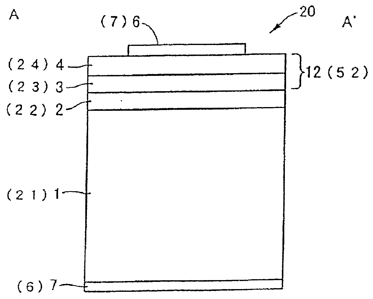
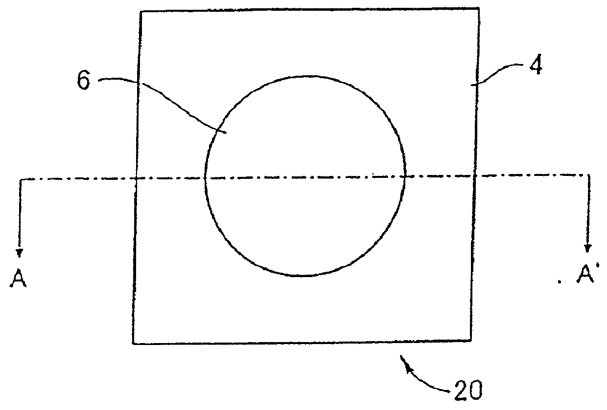
[0069] FIG. 1 is a schematic plan view of a gallium nitride (GaN)-based blue LED having a light-emitting part structure of single hetero (SH) structure containing a gallium nitride phosphide crystal layer. FIG. 2 is a schematic sectional view cut along the line A-A' of FIG. 1, showing a multilayer structure of gallium nitride (GaN)-based blue LED shown in FIG. 1.

[0070] An epitaxial multilayer structure having a light-emitting part structure 12 of single hetero-junction structure was constructed by stacking layers on the surface of a single crystal substrate 1 comprising a p-type silicon having a (100) plane azimuth and having added thereto boron (B), by respective vapor phase growth methods described in the following items (1) to (3).

[0071] (1) A low-temperature buffer layer 2 comprising Zn-doped p-type boron phosphide (BP) was deposited using a mixed gas of triethyl borane ((C.sub.2H.sub.5).sub.3B) / phosphine (PH.sub.3) / hydrogen (H.sub.2) as the starting material gas. The layer was ...

example 2

[0088] In this Example, the present invention is described by referring to a group-III nitride semiconductor light-emitting device having a light-emitting part structure of double hetero (DH) structure containing a gallium nitride phosphide single crystal layer.

[0089] FIG. 3 is a schematic sectional view of a gallium nitride (GaN)-based blue LED fabricated based on a multilayer structure having a light-emitting part structure of DH structure according to the present invention.

[0090] In FIG. 3, the same constituent elements as in FIG. 2 are indicated by the same reference numbers and not described here.

[0091] On the same silicon single crystal substrate 1 as used in Example 1, a BP low-temperature buffer layer 2 was stacked and thereon, a lower clad layer 3 comprising GaN.sub.0.97P.sub.0.03 single crystal was stacked. On this lower clad layer, respective crystal layers described in the following items (1) and (2) were stacked to construct a multilayer structure.

[0092] (1) A light emi...

example 3

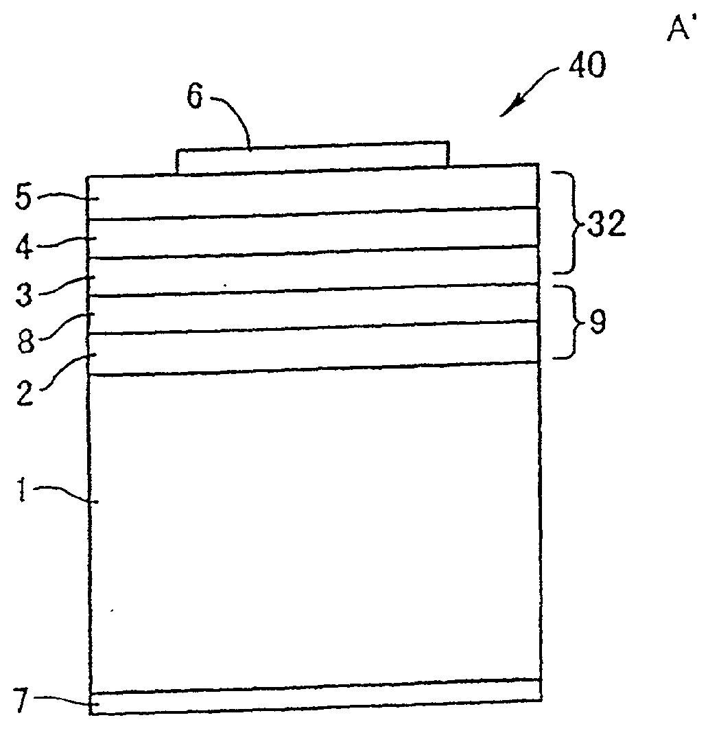
[0109] In this Example, the present invention is described by referring to a group-III nitride semiconductor blue light-emitting device having a DH junction light-emitting part structure containing a gallium nitride phosphide single crystal layer stacked on a buffer layer of a double layer structure.

[0110] FIG. 4 is a schematic sectional view of a gallium nitride-based LED fabricated based on a multilayer structure having a light-emitting part structure of DH structure according to the present invention. In FIG. 4, the same constituent elements as in FIG. 1 are indicated by the same reference numbers and not described here.

[0111] A low-temperature buffer layer 2 comprising boron phosphide (BP) was formed on a silicon single crystal substrate 1 under the growth conditions described in Example 1. On the low-temperature buffer layer 2, a crystalline buffer layer 8 comprising a zinc (Zn)-doped p-type boron phosphide (BP) crystal layer was stacked. The crystalline buffer layer 8 comprisi...


PUM


Abstract

A high emission intensity group-III nitride semiconductor light-emitting device obtained by eliminating crystal lattice mismatch with substrate crystal and using a gallium nitride phosphide-based light emitting structure having excellent crystallinity. A gallium nitride phosphide-based multilayer light-emitting structure is formed on a substrate via a boron phosphide (BP)-based buffer layer. The boron phosphide-based buffer layer is preferably grown at a low temperature and rendered amorphous so as to eliminate the lattice mismatch with the substrate crystal. After the amorphous buffer layer is formed, it is gradually converted into a crystalline layer to fabricate a light-emitting device while keeping the lattice match with the gallium nitride phosphide-based light-emitting part.

Description

[0001] This application is an application filed under 35 U.S.C. .sctn.111(a) claiming benefit pursuant to 35 U.S.C. .sctn.119(e)(1) of the filing date of Provisional Application 60 / 247,989 filed Nov. 14, 2000 pursuant to 35 U.S.C. .sctn.111(b).[0002] The present invention relates to a group-III nitride semiconductor light-emitting device comprising a substrate such as silicon (Si) having on the surface thereof a light-emitting part structure containing a gallium nitride phosphide (GaN.sub.1-XP.sub.X, wherein 0<X<1) single crystal layer provided via a boron phosphide (BP)-based buffer layer.[0003] A group-III nitride semiconductor light-emitting device that emits light in the blue or green band is composed of a multilayer structure where a gallium nitride (GaN) crystal layer as one constituent element is disposed, for example, on a sapphire (.alpha.-Al.sub.2O.sub.3) single crystal substrate using a growing technique, such as metal organic chemical vapor deposition (MOCVD) metho...

Claims


Application Information

Patent Timeline
IPC IPC(8): H01L33/00H01L33/32
CPCH01L33/007H01L33/0075H01L33/32
Inventor UDAGAWA, TAKASHI
Owner SHOWA DENKO KK
Why Eureka
Try Eureka