Plasmon assisted enhancement of organic optoelectronic devices

a technology of optoelectronic devices and plasmons, which is applied in the direction of solid-state devices, thermoelectric devices, material nanotechnology, etc., can solve the problems of limited performance of leds, low luminescence yield, and small oscillator strengths of radiative transition, and achieve enhanced radiative relaxation, enhanced emission properties, and enhanced effect of plasmon enhancemen

Inactive Publication Date: 2005-02-17
RGT UNIV OF CALIFORNIA
View PDF1 Cites 91 Cited by
  • Summary
  • Abstract
  • Description
  • Claims
  • Application Information

AI Technical Summary

Benefits of technology

The present invention provides, inter alia, the surface plasmon-enhancement of organic triplet emitter-based LEDs. It provides optoelectronic devices having enhanced and controllable rates of the radiative relaxation of triplet light emitters, exemplified by organic light emitting devices based on phosphorescent materials with enhanced emission properties. It achieves acceleration of the radiative processes by the interaction of the light emitting species with surface plasmon resonances in the vicinity of metal surfaces. It efficiently suppresses non-radiative Förster-type processes by introducing a transparent dielectric or molecular layer between the metal surface and the chromophore. For materials with low emission oscillator strengths (such as triplet emitters), the optimal separation distance from the metal surface is determined, thus suppressing energy transfer and achieving a significant acceleration of the emission rate.
In order to accelerate the radiative recombination rate of long-living chromophores while preserving their emissive properties, the metal surface and the light emitting species are separated spatially. This prevents emission quenching by Förster-type energy transfer from the fluorophore to the metal. It is possible to determine a critical distance between metal structure supporting surface plasmons and the light emitting molecule. At distances larger than the critical distance but within the plasmon coupling range, the excited state decay of chromophore occurs mostly through radiative channels with a net emission rate higher than that of an isolated molecule. At distances shorter than critical distance, light emission is diminished due to energy transfer processes which destroy the excited states. The critical distance depends on metal nanostructure size, shape, and composition, and is directly proportional to the fluorophore's emissive oscillator strength.
The surface plasmon-assisted radiative decay acceleration is possible both for electrical and optical excitation of fluorescence and phosphorescence. Other techniques for generation of chromophore's excited states are also possible. The present invention enables one to increase the emission quantum yield of the chromophore and to create light emitting devices with improved current conversion efficiency, enhanced brightness, and higher saturation current densities. The increase of light emitting device efficiency is attributed to enhanced emission yield, decreased emission saturation threshold, and local field enhancement effects.

Problems solved by technology

However, such materials typically exhibit small oscillator strengths of the radiative transition and very long emission life-times (up to several seconds).
This leads to low luminescence yields due to competition with faster non-radiative processes.
Also, slow radiative recombination limits the performance of LEDs due saturation of lumophores and non-radiative processes such as triplet-triplet quenching, at high rates of carriers injection.
Third, the chromophore's interactions with metal surfaces can introduce additional non-radiative losses caused by Förster-type energy transfer between the emitter and a metal [Lakowicz; Weissberger et al.].
The latter process leads to quenching of light emission, and could significantly degrade the luminescence yield.
For singlet emitting chromophores, with high oscillator strength, efficient energy transfer makes the enhancement difficult.
Several attempts have been made to alter the decay rate in singlet emitters [Lakowicz], but were inconclusive since acceleration of the excited state decay in this case could be attributed to fast quenching processes.

Method used


Image

  • Plasmon assisted enhancement of organic optoelectronic devices
  • Plasmon assisted enhancement of organic optoelectronic devices
  • Plasmon assisted enhancement of organic optoelectronic devices

Examples


example 1

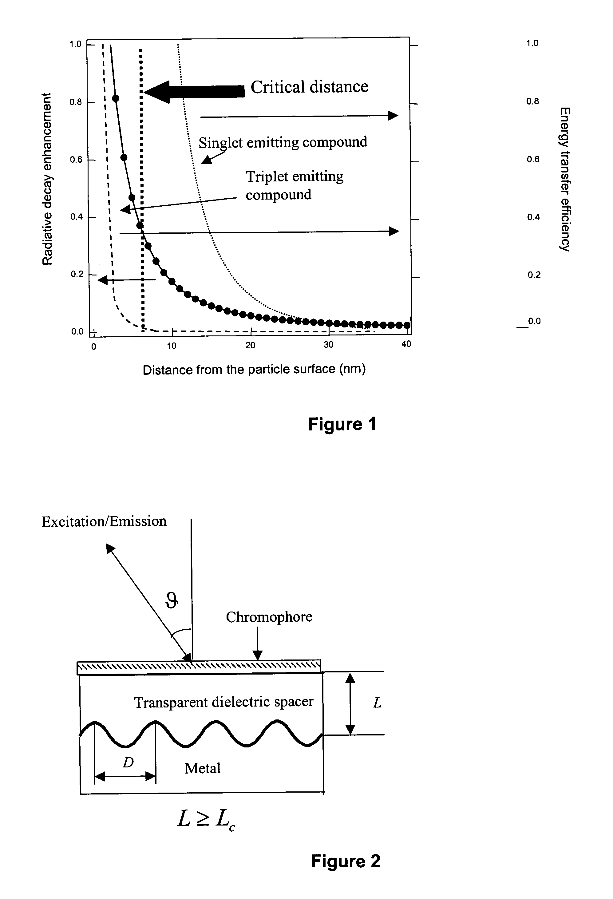
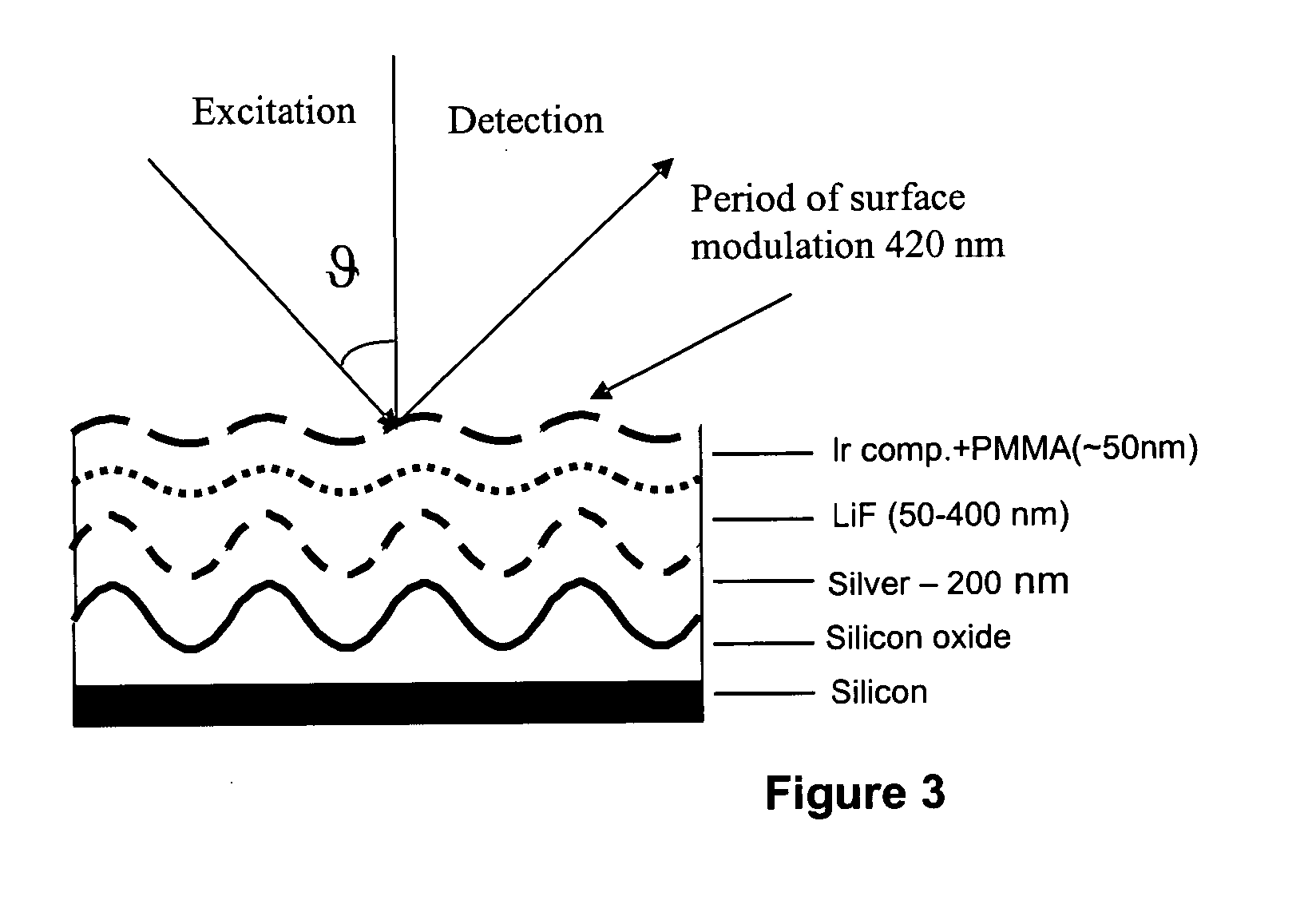
FIG. 3 depicts a planar metal structure with periodic modulation and dielectric spacer layer separating a metal surface and chromophore. It shows the layout of a planar periodic structure designed and constructed to demonstrate surface plasmon-assisted acceleration of radiative processes in triplet chromophores. The structure comprises a silver grating coated with a lithium fluoride, LiF, layer of variable thickness and a layer of iridium triplet emitter on top. The substrate was made by oxidizing a silicon wafer and then introducing a holographic grating with a 440 nm periodic structure and an amplitude of 70 nm, by photolithographic means. On this grating, a 200 nm sliver film was formed by e-beam deposition techniques. To avoid oxidation of the silver surface, substrates were placed under a nitrogen atmosphere before e-beam deposition of LiF films. The LiF thickness varied between 2-400 nm to change the average distance between the chromophores and the silver surface and to find ...

example 2

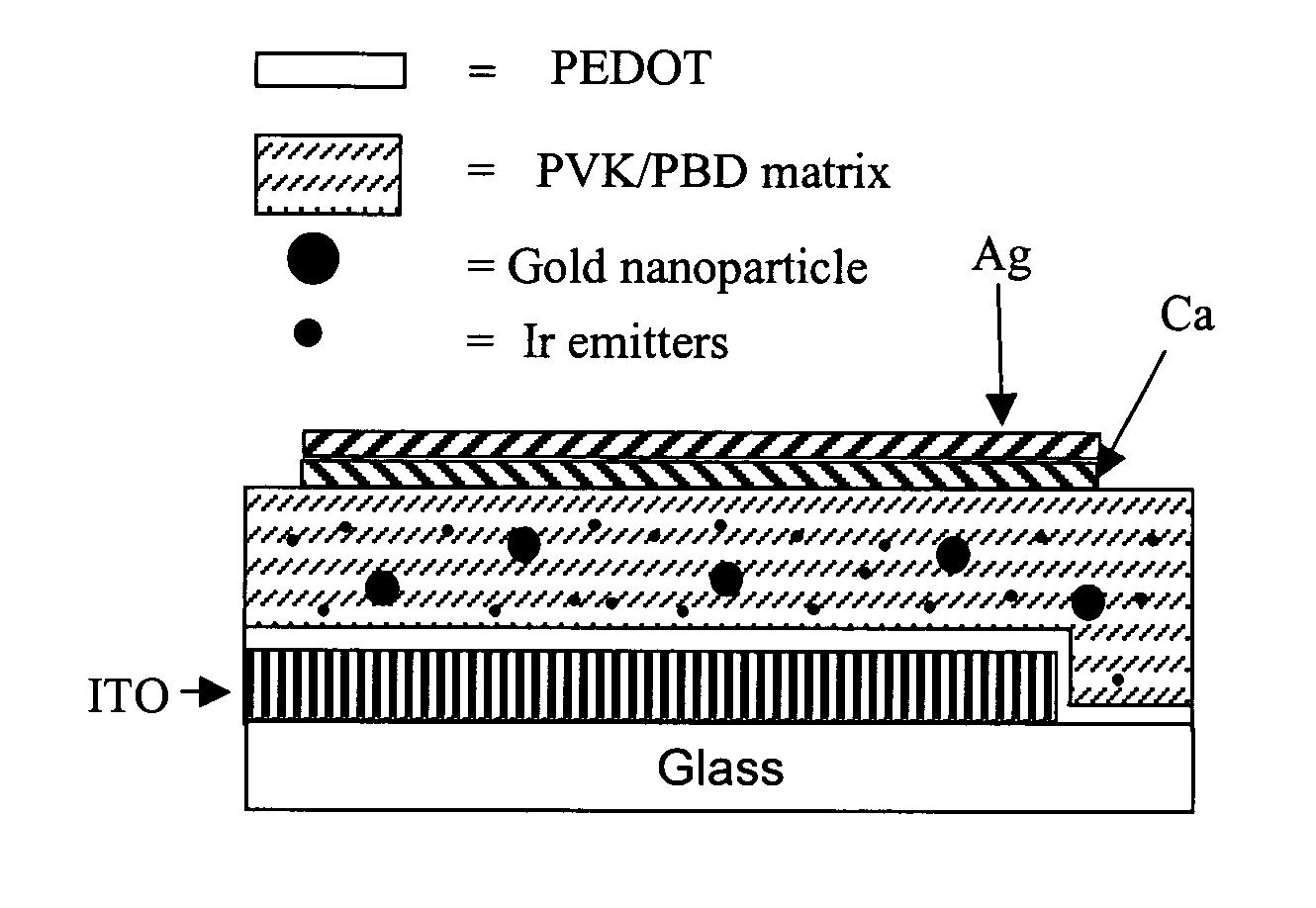
In this example, gold colloidal nanoparticles were embedded in OLEDs in order to enhance device efficiency and increase the saturation threshold of triplet emitters under a large charge injection rate.

Au nanoparticles were synthesized according to Brust et al. HAuCl4 in H2O (15 mL) was added into a reaction vessel. To this tetra octyl ammonium bromide (TOABr) in 40 mL toluene was added and stirred for 20 minutes. Dodecylthiol was added subsequently to serve as a capping agent and to provide a spacer layer of organic molecules around the nanoparticle's core and prevent non-radiative emission quenching. After an additional 20 minutes of stirring, NaBH4 was added, the reaction mixture turned black, and this was stirred for an additional 1.5 hours. The aqueous phase was removed and the organic phase was washed with 1 M H2SO4, concentrated sodium bicarbonate, and dried with sodium sulfate. The particles were precipitated with methanol, MeOH, and the suspension was centrifuged to colle...


PUM


Abstract

Optoelectronic devices and methods for their fabrication having enhanced and controllable rates of the radiative relaxation of triplet light emitters are provided exemplified by organic light emitting devices based on phosphorescent materials with enhanced emission properties. Acceleration of the radiative processes is achieved by the interaction of the light emitting species with surface plasmon resonances in the vicinity of metal surfaces. Non-radiative Förster-type processes are efficiently suppressed by introducing a transparent dielectric or molecular layer between the metal surface and the chromophore. For materials with low emission oscillator strengths (such as triplet emitters), the optimal separation distance from the metal surface is determined, thus suppressing energy transfer and achieving a significant acceleration of the emission rate.

Description

FIELD OF THE INVENTION The present invention is in the field of organic optoelectronic devices, particularly electroluminescent organic light emitting diodes. BACKGROUND OF THE INVENTION The basic structure of an organic light emitting diode (OLED) consists of a stack of thin layers of organic material sandwiched between a transparent anode and a metallic cathode. The organic material layers comprise a hole-injection layer, a hole-transport layer, an emissive layer, and an electron-transport layer. When an appropriate voltage (typically between 2 and 30 volts) is applied to the device, the injected charge excites the chromophores to produce light (electroluminescence) by the radiative recombination of injected positive and negative charges in the emissive layer. The structure of the organic layers and the anode and cathode are chosen to maximize the radiative recombination process in the emissive layer, thus maximizing the light output from the OLED device. Similar devices are pol...

Claims


Application Information

Patent Timeline
Patent Type & Authority Applications(United States)
IPC IPC(8): H01L35/24H01L51/50H01L51/52
CPCB82Y20/00H01L51/5262H01L51/5016B82Y30/00H10K50/11H10K2101/10H10K50/85
Inventor BAZAN, GUILLERMO C.OSTROWSKI, JACEKMIKHAILOVSKY, ALEXANDERKATIYAR, MONICA
Owner RGT UNIV OF CALIFORNIA
Why Eureka
Try Eureka