Sintered diamond having high thermal conductivity and method for producing the same and heat sink employing it

a technology diamond, which is applied in the field of high thermal conductivity composite materials, can solve the problems of thermal management, thermal conductivities of these materials (250 w/mk for ain and 270 w/mk for sic), and thermal stress caused by mismatch, so as to prolong the life of the semiconductor. the effect of improving the performance of the semiconductor chip

Active Publication Date: 2005-03-10
SUMITOMO ELECTRIC IND LTD
View PDF21 Cites 45 Cited by
  • Summary
  • Abstract
  • Description
  • Claims
  • Application Information

AI Technical Summary

Benefits of technology

Thus, by applying the diamond compact of the present invention to a heat sink material, a high performance heat sink with at least one side of at least 3 mm for mounting a semiconductor chip, which has been hard to realize due to the mismatch of CTEs between the semiconductor chip and the heat sink, can be provided. This heat sink, in particular, has remarkable advantages of the improvement of the performance of the semiconductor chips or the extension of the semiconductor life when at least one side of the semiconductor chip is at least 1 mm. That is, the merits of the present invention are particularly remarkable when the size of the heat sink is at least 3 mm square.

Problems solved by technology

Thermal management is a critical issue in electronic parts such as the semiconductor lasers for optical communications and a high performance MPU.
In recent years, however, the thermal conductivities of these materials (250 W / mK for AIN and 270 W / mK for SiC) are getting insufficient to remove the generated heat from the electronic components because the more heat is being generated by the electronic parts as the output power of semiconductor lasers or the integration level of ICs is getting higher.
To meet this requirement, the semiconductor laser chips get larger in sizes and thus the thermal stress caused by the mismatch of the coefficient of thermal expansion (hereinafter referred to as CTE) between the semiconductor chips and the heat sinks gets a serious problem.
More specifically, as the CTE of diamond is about 2.3×10⁻⁶ / K and is much smaller than that of GaAs (5.9×10⁻⁶ / K) or of InP (4.5×10⁻⁶ / K), the reliability of the diode lasers is limited by the operation cycles as well as the soldering process.
Unfortunately, this composite material has some problems.
One is the insufficient thermal conductivity because of the remaining voids within the composite caused by the poor wettability and reactivity between diamond and metals such as copper, silver, gold and aluminum.
In addition to that because of the poor reactivity between diamond and the said metals, the surface roughness of the finished products is not smooth enough due to the removal of diamond particles from the surface during surface polishing process.
The poor surface roughness of the heat sink makes the thermal contact between the semiconductor chip and the heat sink weak and thus the heat sink can not remove the heat efficiently enough.
Typical powder metallurgy techniques, however, have the same problems as those of JP-A-2-170452.
According to this method, however, the metal carbide at the interface degrades the thermal conductivity and a material of higher thermal conductivity cannot be obtained when compared with a material consisting of only diamond and copper.
Moreover, the thermal conductivity of the compact is at most 400 W / mK by the adverse effect of the binder metal whose thermal conductivity is rather low.
By this method, however, one cannot obtain a diamond compact having thermal conductivity as high as 500 W / mK due to the small amount of oxidization of copper during the sintering process in which the capsule is partly broken under pressure and some leak of air occurs.
As above described, in the prior art, there have been no high performance heat sink materials suitable for high power semiconductor laser diodes or high performance MPUs due to the large mismatches of CTE between the conventional high thermal conductivity heat sink materials and semiconductor materials or due to the surface roughness of the polished surface.

Method used


Image

  • Sintered diamond having high thermal conductivity and method for producing the same and heat sink employing it
  • Sintered diamond having high thermal conductivity and method for producing the same and heat sink employing it
  • Sintered diamond having high thermal conductivity and method for producing the same and heat sink employing it

Examples


example 1

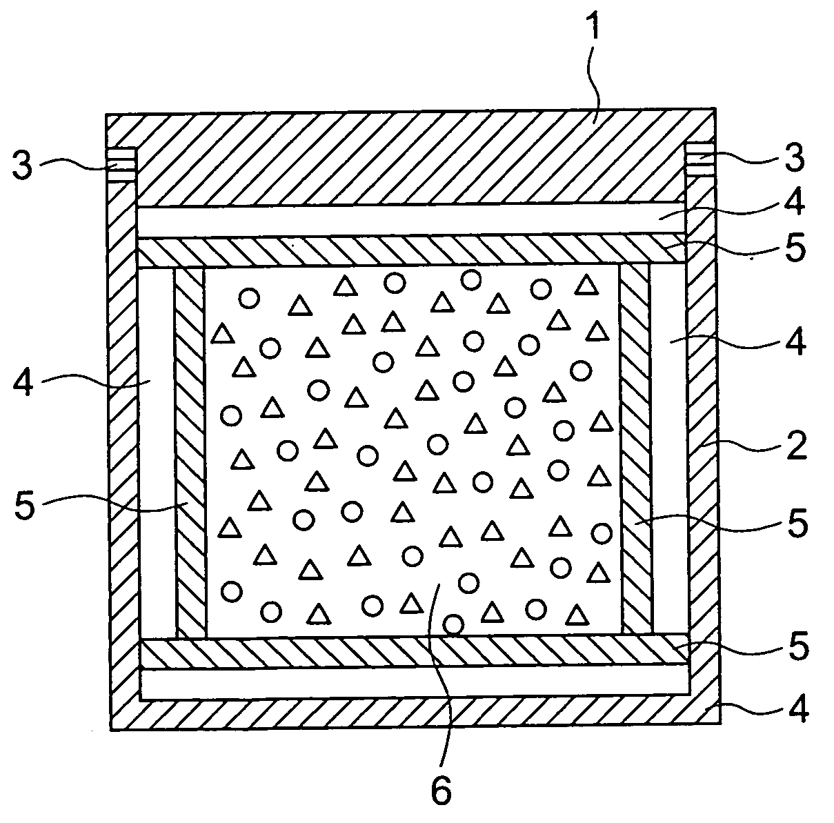
A commercially available diamond powder having a required grain diameter as shown in Table 1 and a copper powder having a grain diameter of at most 15 μm and a purity of 99.9% is mixed with a mixing ratio of Table 1, the mixed powders were charged in a container made of molybdenum, having such a construction as shown in FIG. 6, and an inner diameter of 25 mm and a depth of 5 mm with a niobium plate and titanium plate and compressed at a load of 2 t / cm2 to obtain a compressed powder body. The container charged with this compressed body was covered with a molybdenum lid through a brazing material and heated in vacuum to braze and seal the container and lid. As comparative examples, there are shown in Table 1, as Comparative Examples 1 to 16, in which diamond grains having grain diameter of less than 5 μm were charged in the same capsule, or diamond grains having grain diameter of 5 to 100 μm were charged without vacuum sealing or without titanium plate and were prepared in the simila...

example 2

A commercially available diamond powder having a required grain diameter as shown in Table 1 was charged in a container made of molybdenum, having an inner diameter of 25 mm and a depth of 5 mm and compressed at a load of 2 t / cm2 to obtain a compressed powder body of 2 mm thick. An oxygen free copper plate having a diameter of 25 mm and thickness of 0.5 mm was arranged to be in contact with the compressed body, upon which a Zr foil having a diameter of 25 mm and thickness of 0.5 mm was arranged. The container charged as described above, was covered with a molybdenum lid through a brazing material and heated in vacuum to braze and seal the container and lid. As comparative examples, there are shown in Table 2, as Comparative Examples 17 to 18, in which diamond grains were charged without vacuum sealing or without zirconium plate and were prepared in the similar step and the like.

These containers were charged in an ultra-high pressure producing apparatus belt type, maintained at a ...

example 3

The sintered compact prepared in Example 1 was worked so as to give a thickness of 0.5 mm by discharge working and then subjected to lapping at both the surface and back surface by the use of a diamond wheel of # 400. The thus lapped sintered compact was cut in a dimension of 3 mm×1 mm using a YAG laser having an output of 3 W. After the cutting work, breakages at the cutting edge and the surface roughnes of the lapped surface were measured to obtain results shown in Table 3. Similarly, a sample with a diamond grain diameter of 110 μm (Comparative Example 14) and another sample with a diamond grain diameter of 130 μm (Comparative Example 15), as comparative examples, were sintered in an analogous manner to Example 1 and then subjected to a working test, thus obtaining results shown in the same table.

TABLE 3SurfaceMaximum BreakageRoughnessQuantity at EndSample No.(Ra: μm)(μm)10.08820.07830.07640.06550.05460.05370.03280.012Comparative0.1210 Example 14Comparative0.1512 Example 15


PUM

PropertyMeasurementUnit
grain size distributionaaaaaaaaaa
densityaaaaaaaaaa
densityaaaaaaaaaa

Abstract

This invention relates to a high thermal conductivity composite material which comprises diamond particles and a copper matrix useful as electronic heat sinks for electronics parts, particularly for semiconductor lasers, high performance MPUs (micro-processing units), etc., also to a process for the production of the same and a heat sink using the same. According to the high thermal conductivity diamond sintered compact of the present invention, in particular, there can be provided a heat sink having a high thermal conductivity as well as matching of thermal expansions, most suitable for mounting a large sized and high thermal load semiconductor chip, for example, high output semiconductor lasers, high performance MPU, etc. Furthermore, the properties such as thermal conductivity and thermal expansion can freely be controlled, so it is possible to select the most suitable heat sink depending upon the features and designs of elements to be mounted.

Description

FIELD OF THE INVENTION This invention relates to a high thermal conductivity composite material which comprises diamond particles and a copper matrix useful as electronic heat sinks for electronics parts, particularly for semiconductor lasers, high performance MPUs (micro-processing units), etc., also to a process for the production of the same and a heat sink using the same. BACKGROUND OF THE INVENTION Thermal management is a critical issue in electronic parts such as the semiconductor lasers for optical communications and a high performance MPU. In most cases efficient removal of the heat generated by the semiconductor component is achieved by directly bonding a semiconductor component on a heat sink with a solder. In the prior art an aluminum nitride (AIN) compact or a silicon carbide (SiC) compact has been the widely used material for the heat sinks above mentioned. In recent years, however, the thermal conductivities of these materials (250 W / mK for AIN and 270 W / mK for SiC)...

Claims


Application Information

Patent Timeline
Patent Type & Authority Applications(United States)
IPC IPC(8): C04B35/645H01L23/373
CPCC04B35/52Y10T428/2982C04B35/645C04B2235/3817C04B2235/3826C04B2235/3839C04B2235/404C04B2235/405C04B2235/407C04B2235/427C04B2235/428C04B2235/723C04B2235/77C04B2235/786C04B2235/80C04B2235/9607H01L23/3732H01S5/02476H01L2924/0002Y10S438/929C04B35/62842Y10T428/30Y10T428/26H01L2924/00
Inventor YOSHIDA, KATSUHITOMORIGAMI, HIDEAKIAWAJI, TAKAHIRONAKAI, TETSUO
Owner SUMITOMO ELECTRIC IND LTD
Why Eureka
Try Eureka