Highly crystalline aluminum nitride multi-layered substrate and production process thereof

a technology of aluminum nitride and multi-layered substrate, which is applied in the direction of solid-state diffusion coating, after-treatment details, superimposed coating process, etc., can solve the problems of large distortion at the bonding boundary, difficult to obtain homogeneous thin films without defects, and difficult to obtain group iii nitride thin films with few defects, etc., to achieve excellent crystallinity, low dislocation density, and low dislocation density

Inactive Publication Date: 2005-03-17
TOKYO INST OF TECH +1
View PDF6 Cites 23 Cited by
  • Summary
  • Abstract
  • Description
  • Claims
  • Application Information

AI Technical Summary

Benefits of technology

In the present invention, by nitriding the surface of a single-crystal α-alumina substrate, for example, a sapphire substrate, an alon layer is formed on the surface and a highly crystalline AlN film is formed on this alon layer as the under layer as described above. Therefore, the obtained alon layer has an extremely low dislocation density and multi-layer defect density and excellent crystallinity and the AlN film also has a low dislocation density and excellent crystallinity.
Therefore, when this highly crystalline AlN film is used as a light emitting device, an ultraviolet light emitting device having extremely high light emission efficiency can be obtained, and it can be used in a high-density optical memory and also other various fields as an ultraviolet light receiving device. Further, when a group III nitride semiconductor typified by GaN is epitaxially grown on this highly crystalline AlN film, a highly crystalline group III nitride semiconductor film having extremely high crystallinity and few defects can be formed. Therefore, the light emission efficiency of a blue light emitting device or ultraviolet light emitting device comprising this highly crystalline group III nitride semiconductor film can be significantly improved. Further, the highly crystalline AlN film can also be used as a surface acoustic wave device and the drive efficiency of a surface acoustic wave device comprising the film can be improved.

Problems solved by technology

However, as its lattice mismatch with a substrate material is large, it is still extremely difficult to obtain a group III nitride thin film having few defects.
However, as the buffer layer of AlN itself has a large lattice mismatch with the sapphire substrate, it is difficult to obtain a homogeneous thin film having no defect.
In all of these methods, great distortion remains at the bonding boundary due to a large lattice mismatch between the sapphire of the substrate and the AlN thin film.
Accordingly, the conventional AlN film does not fully serve as a buffer layer for growing a GaN film, and threading dislocations are existent in the GaN film from the substrate to the surface of the film at a density of 108 / cm2 or more.
This is the cause of reducing the light emission efficiency of a light emitting device.
Therefore, it cannot be said that the lattice mismatch is fully improved.

Method used


Image

  • Highly crystalline aluminum nitride multi-layered substrate and production process thereof
  • Highly crystalline aluminum nitride multi-layered substrate and production process thereof
  • Highly crystalline aluminum nitride multi-layered substrate and production process thereof

Examples


example 1

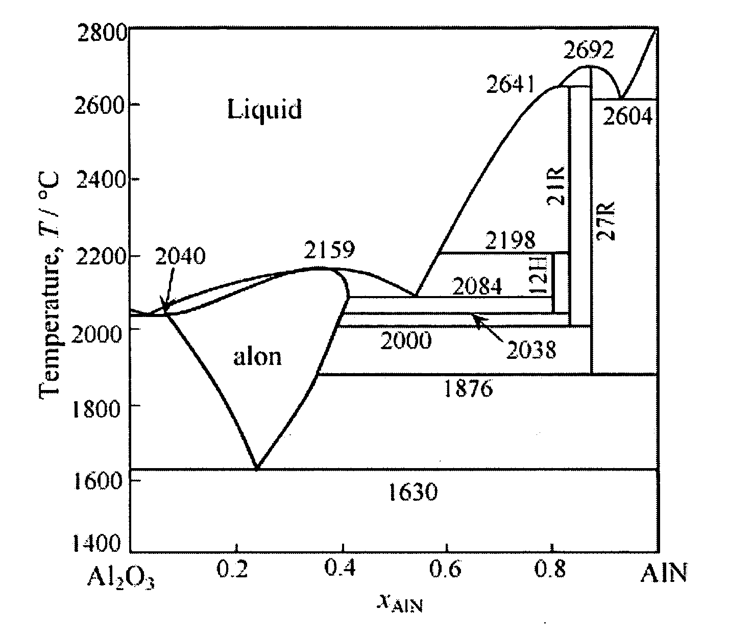
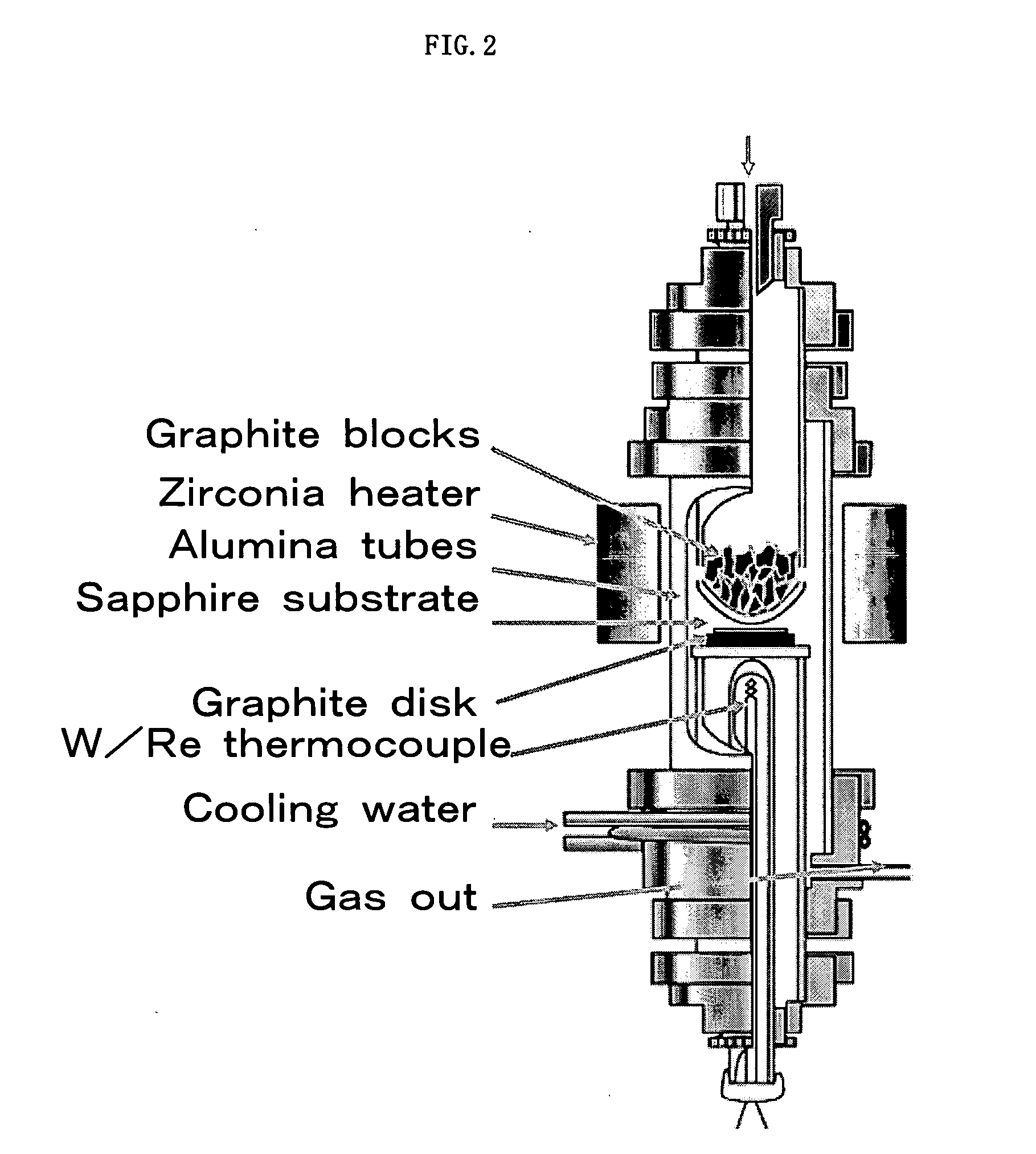
An AlN film and an alon layer were formed by nitriding a sapphire substrate with an N2—CO mixed gas and graphite at 1,690° C. in the reactor shown in FIG. 2. An alumina base was installed at the center of an alumina reaction tube, and a graphite disk (purity of 99.999%, 15 mm in diameter×2.5 mm) and a sapphire substrate (12.5 mm in diameter×0.33 mm) whose surface crystal plane was the (11-20) plane, face A, were mounted on the base. The sapphire substrate before a reaction had a surface roughness Ra of less than 1 nm and a half-value width of its rocking curve of 56 arcsec. A one-end closed pipe having four 2 mm-diameter holes in the bottom in a horizontal direction was inserted above the sapphire substrate, 5.0 g of graphite blocks (purity of 99.999%) were filled in the pipe, and a mixed gas to be introduced passed through this graphite layer to reach the sample.

The inside of the reaction tube was evacuated with a rotary pump to completely remove water in the tube and completely...

example 2

An AlN film and an alon layer were formed by nitriding a sapphire substrate with a N2—CO mixed gas and graphite at 1,660° C. in the reactor shown in FIG. 2. The details of the reactor were the same as in Example 1 and a mixed gas having a partial pressure ratio of carbon monoxide (CO) to nitrogen (N2) of 0.1 was introduced to maintain the inside of the reactor at 1,660° C. for 24 hours.

The crystal orientation relationship between the obtained alon layer and AlN film was completely the same as in Example 1.

FIG. 9 shows graphs of ω-mode rocking curves. It is understood from the graphs that as the half-value width of the alon layer was 4,320 arcsec and the half-value width of AlN was 281 arcsec, they have high crystallinity. The half-value width of the sapphire substrate after the reaction was 241 arcsec.

FIG. 10 is a TEM image of the cross sections of the AlN film and alon layer formed on the face-A sapphire substrate obtained in this example. It is understood from this image and ...


PUM

PropertyMeasurementUnit
Raaaaaaaaaaa
equilibrium partial pressureaaaaaaaaaa

Abstract

A highly crystalline aluminum nitride multi-layered substrate comprising a single-crystal α-alumina substrate, an aluminum oxynitride layer and a highly crystalline aluminum nitride film as the outermost layer which are formed in the mentioned order, wherein
    • the aluminum oxynitride layer has a threading dislocation density of 6.3×10⁷/cm2 or less and a crystal orientation expressed by the half-value width of its rocking curve of 4,320 arcsec or less; and a production process thereof.

Description

FIELD OF THE INVENTION The present invention relates to a highly crystalline aluminum nitride multi-layered substrate comprising a highly crystalline aluminum nitride (AlN) film as the outermost layer and a production process thereof. DESCRIPTION OF THE PRIOR ART A group III nitride semiconductor typified by gallium nitride (GaN) is attracting much attention as a light emitting device such as a light emitting diode (LED) or laser which emits blue to ultraviolet light. A group III nitride having a high melting point must be epitaxially grown on a substrate such as a sapphire substrate as seen in the multi-layered structure of a blue LED. However, as its lattice mismatch with a substrate material is large, it is still extremely difficult to obtain a group III nitride thin film having few defects. Since the light emission efficiency of a group III nitride-based semiconductor device is determined largely by initial crystal growth on a substrate, the development of a substrate material...

Claims


Application Information

Patent Timeline
Patent Type & Authority Applications(United States)
IPC IPC(8): C23C8/24C23C8/28C23C28/04C30B29/20C30B29/38C30B33/00H01L21/00H01L21/302H01L21/461H01L21/84
CPCC23C8/24C23C8/28C30B33/00C30B29/38C30B29/20
Inventor FUKUYAMA, HIROYUKINAKAO, WATARUKUSUNOKI, SHINYATAKADA, KAZUYAHAKOMORI, AKIRA
Owner TOKYO INST OF TECH
Why Eureka
Try Eureka