
Visible/near infrared image sensor

a technology of infrared image and sensor, which is applied in the field of image sensors, can solve the problems of limiting the achievable pixel count, low collection efficiency, and limited photoresponse of these sensors, and achieves enhanced sensitivity, pixel size and pixel count, and low electrical bias voltage.

Inactive Publication Date: 2005-05-19
C PHOCUS
View PDF6 Cites 144 Cited by
  • Summary
  • Abstract
  • Description
  • Claims
  • Application Information

AI Technical Summary

Benefits of technology

[0009] The present invention provides a MOS or CMOS sensor for high performance imaging in broad spectral ranges including portions of the infrared spectral band. These broad spectral ranges may also include portions or all of the visible spectrum, therefore the sensor has both daylight and night vision capabilities. The sensor includes a continuous multi-layer photodiode structure on a many pixel MOS or CMOS readout array where the photodiode structure is chosen to include responses in the near infrared spectral ranges. A preferred embodiment incorporates a microcrystalline copper indium diselenide/cadmium sulfide photodiode structure on a CMOS readout array. An alternate preferred embodiment incorporates a microcrystalline silicon germanium photodiode structure on a CMOS readout array. Each of these embodiments provides night vision with image perf

Problems solved by technology

The photoresponse of these sensors is typically limited to the 400 nm-900 nm spectral range by the semiconductor bandgap properties of crystalline silicon.
Also, in prior art CMOS sensors, the CMOS pixel circuitry obscures a major portion of each pixel's photosensitive area, resulting in low collection efficiency.
Bump bonding requires fairly large pixel sizes (typically 25-50 microns); this limits the achievable pixel count.
These devices require a vacuum and a high applied voltage (200 V-800 V) which results in bulky packaging and increased risk of damage.
The 15 micron micro-channel spacing results in relatively large effective pixel sizes, which limits the pixel count.

Method used


Image

  • Visible/near infrared image sensor
  • Visible/near infrared image sensor
  • Visible/near infrared image sensor

Examples


Embodiment Construction

Two Million Pixel CMOS Sensor

General Description

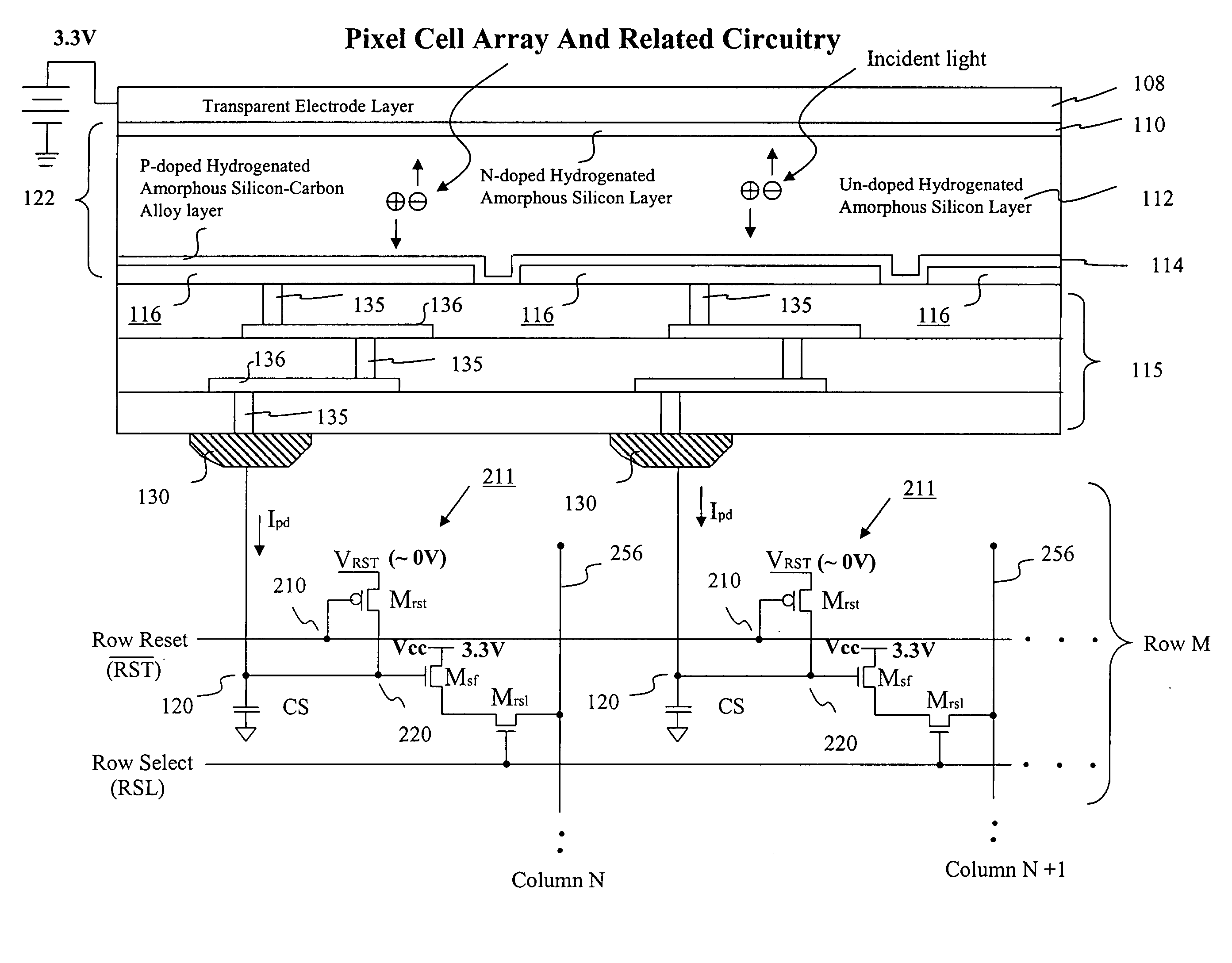
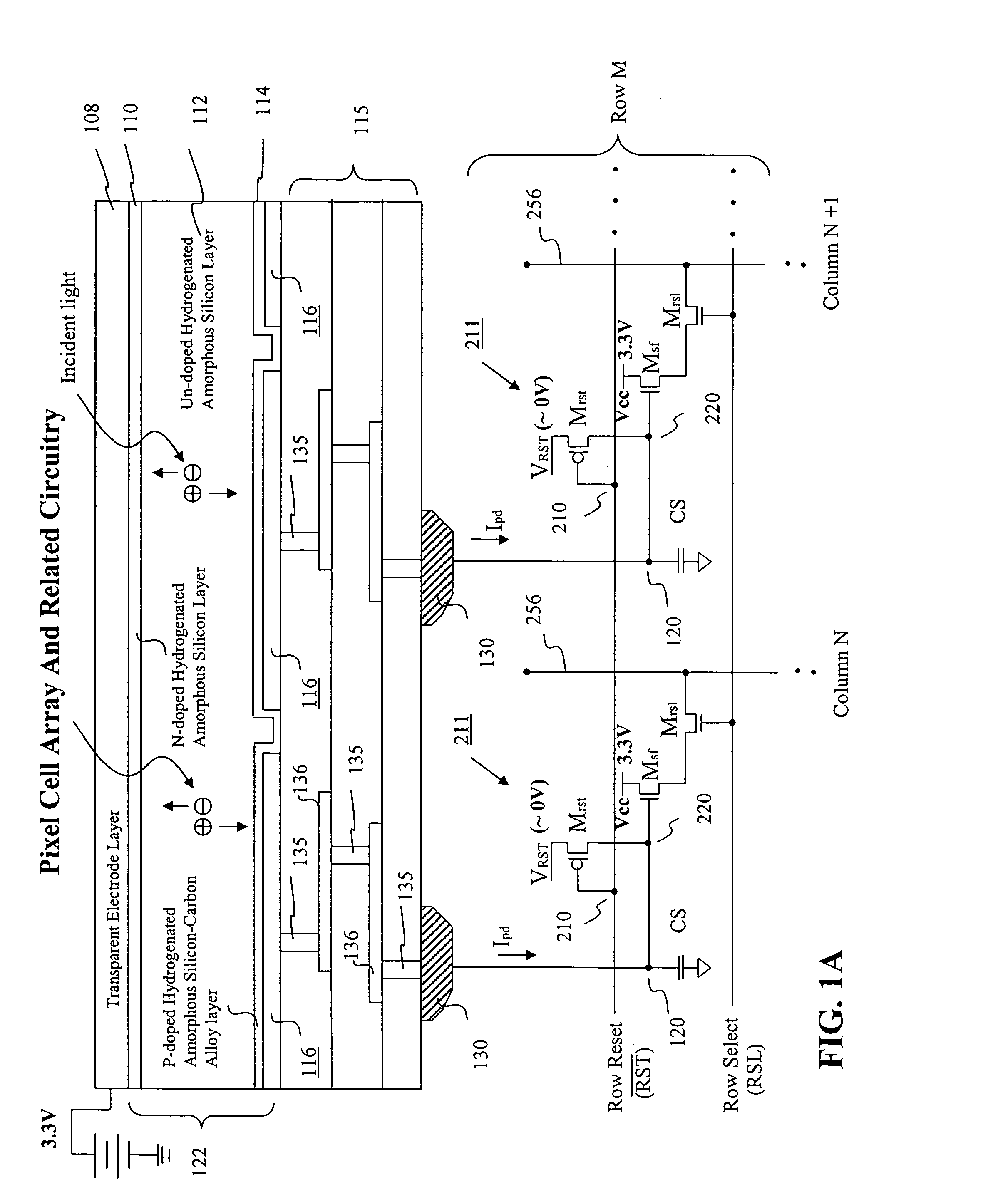
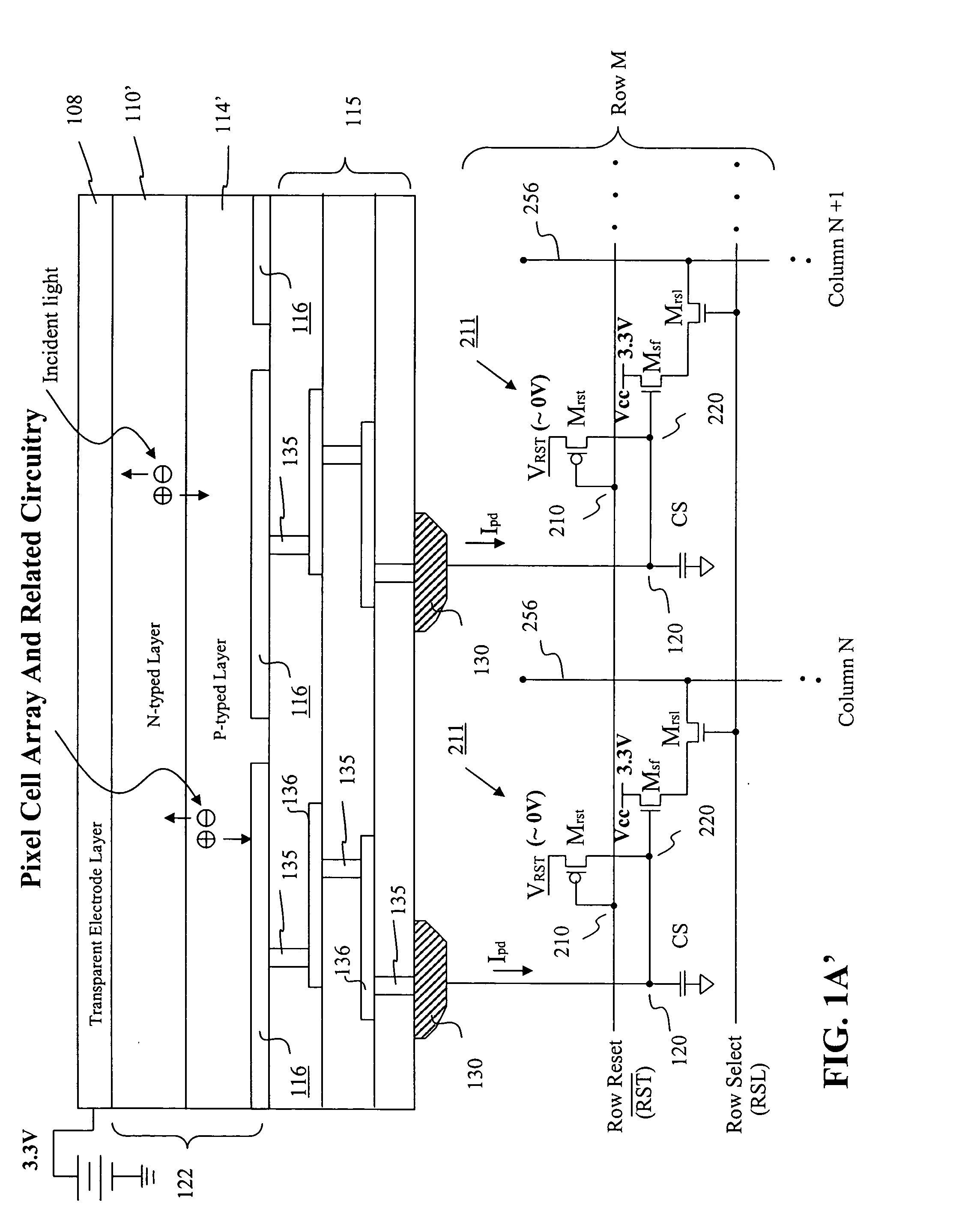
[0031] Some features of a two-million pixel CMOS sensor are shown in FIGS. 1A through 1H. This sensor is fabricated by depositing a multi-layer photodiode structure on top of an electronic readout array that is fabricated using complimentary metal-oxide semiconductor (CMOS) methods commonly utilized in integrated circuit manufacturing. Absorbed photons create charge pairs in the photodiode structure and the liberated electric charge migrates under the influence of an applied electric field to pixel pads in the CMOS readout array where the charges are stored on capacitors, each capacitor representing a pixel. Active pixel circuitry at each pixel produces an amplified voltage proportional to the stored electric charge. CMOS readout circuitry, that may be located at the periphery of each array column, further amplifies and digitizes the pixel signal. Additional pixel circuitry provides digital multiplexing of the digitized pixel signal...


PUM


Abstract

A MOS or CMOS sensor for high performance imaging in broad spectral ranges including portions of the infrared spectral band. These broad spectral ranges may also include portions or all of the visible spectrum, therefore the sensor has both daylight and night vision capabilities. The sensor includes a continuous multi-layer photodiode structure on a many pixel MOS or CMOS readout array where the photodiode structure is chosen to include responses in the near infrared spectral ranges. A preferred embodiment incorporates a microcrystalline copper indium diselenide / cadmium sulfide photodiode structure on a CMOS readout array. An alternate preferred embodiment incorporates a microcrystalline silicon germanium photodiode structure on a CMOS readout array. Each of these embodiments provides night vision with image performance that greatly surpasses the GEN III night vision technology in terms of enhanced sensitivity, pixel size and pixel count. Further advantages of the invention include low electrical bias voltages, low power consumption, compact packaging, and radiation hardness. In special preferred embodiments CMOS stitching technology is used to provide multi-million pixel focal plane array sensors. One embodiments of the invention made without stitching is a two-million pixel sensor. Other preferred embodiments available using stitching techniques include sensors with 250 million (or more) pixels fabricated on a single wafer. A particular application of these very high pixel count sensors is as a focal plane array for a rapid beam steering telescope in a low earth orbit satellite useful for tracking over a 1500-meter wide track with a resolution of 0.3 meter.

Description

[0001] This application is a continuation in part of U.S. patent application Ser. No. 10 / 746,529, filed Dec. 23, 2003; Ser. No. 10 / 648,129 filed Aug. 26, 2003; Ser. No. 10 / 371,618, filed Feb. 22, 2003; Ser. No. 10 / 229,953 filed Aug. 27, 2002; Ser. No. 10 / 229,954 filed Aug. 27, 2002; Ser. No. 10 / 229,955 filed Aug. 27, 2002; Ser. No. 10 / 229,956 filed Aug. 27, 2002 and Ser. No. 10 / 072,637 filed Feb. 5, 2002. This patent application relates to image sensors and in particular to broad spectrum image sensors covering spectral ranges within the visible and near infrared spectral ranges.BACKGROUND OF THE INVENTION [0002] The prior art includes a variety of image sensors. Image sensors operating in the visible and near infrared spectrums have widespread utility for military and commercial applications. Charge Coupled Devices [0003] Charge coupled device (CCD) image sensors are pixelated readout arrays fabricated on and in a crystalline silicon substrate. These sensors convert incident light ...

Claims


Application Information

Patent Timeline
IPC IPC(8): H01L27/00H01L27/10H01L27/146H01L29/76H01L31/00H01L31/062H01L31/105H01L31/113
CPCG01J5/02Y02E10/545G01J5/026G01J5/04G01J5/046G01J5/22G01J5/52G01J2005/0077H01L27/14609H01L27/14621H01L27/1463H01L27/14632H01L27/14636H01L27/14643H01L27/14645H01L27/14649H01L27/14687H01L27/14689H01L27/14692H01L31/03685H01L31/03687H01L31/1055H01L31/109H01L31/113H04N3/155H04N5/2351H04N5/2353H04N5/33H04N5/332H04N5/365H04N5/374H04N5/37455H04N5/378Y02E10/548G01J5/024H04N23/71H04N23/73H04N23/11H04N25/67H04N25/671H04N25/772H04N25/76H04N25/75
Inventor ENGELMANN, MICHAEL G.CHAO, CALVINHSIEH, TZU-CHIANGMARTIN, PETERPENDER, MILAM
Owner C PHOCUS
Learn More