Composition for forming silicon film and method for forming silicon film

a technology of silicon film and composition, which is applied in the direction of crystal growth process, polycrystalline material growth, plasma technique, etc., can solve the problems of lowering production yield, complex and expensive high frequency generator and vacuum device, and high cos

Inactive Publication Date: 2005-07-07
JSR CORPORATIOON
View PDF7 Cites 85 Cited by
  • Summary
  • Abstract
  • Description
  • Claims
  • Application Information

AI Technical Summary

Benefits of technology

[0016] Further, secondly, the above object and advantage of the present invention are achieved by a method for forming a silicon film which comprises the steps of forming a coating film of the above silicon-film-forming composition on a substrate and subjecting the coating film to instantaneous fusion, a heat treatment or a light treatment.

Problems solved by technology

However, the formation of the silicon films by these CVD methods has problems that since a gas phase reaction is used, the contamination of equipment and / or production of foreign materials are / is caused by by-production of silicon particles in the gas phase, thereby lowering a production yield, that since the raw material is in gaseous form, it is difficult to form a silicon film having a uniform film thickness on a substrate having an uneven surface, that productivity is low due to a low film formation rate and that complex and expensive high frequency generator and vacuum device are required in the plasma CVD method.
As for the raw material, since gaseous silicon hydride which is highly toxic and reactive is used, it is difficult to handle, and a sealable vacuum device is required since the raw material is in gaseous form.
In general, these devices are large and expensive and also cause an increase in production costs since they consume a large amount of energy for a vacuum system or a plasma system.
However, this method has problems that a complex device is required since gasification and cooling of silicon hydride as the raw material are carried out successively and that it is difficult to control the thickness of the film.
However, this method is difficult to use since the system is unstable, and since the raw material is in liquid form, it is difficult to obtain a uniform film thickness when it is coated on a substrate with a large area.
However, a film cannot be formed by a coating method since the polymer is insoluble in a solvent.
The formation of the silicon film by use of the thermal or plasma CVD method has problems that:
(1) since a gas phase reaction is used, silicon particles are produced in the gas phase and cause the contamination of equipment and / or production of foreign materials, thereby lowering a production yield,
(2) since the raw material is in gaseous form, it is difficult to form a silicon film having a uniform thickness on a substrate having an uneven surface,
(3) productivity is low due to a low film formation rate, and
(4) complex and expensive high frequency generator and vacuum device are required in the plasma CVD method.

Method used


Image

  • Composition for forming silicon film and method for forming silicon film
  • Composition for forming silicon film and method for forming silicon film

Examples


synthesis example 1

[0100] The inside of a 3-liter four-neck flask equipped with a thermometer, a cooling condenser, a dropping funnel and an agitator was substituted with an argon gas. Then, 1 liter of dried tetrahydrofuran and 18.3 g of lithium metal were charged into the flask and bubbled with an argon gas.

[0101] While this suspension was being stirred at 0° C., 333 g of diphenyldichlorosilane was added through the dropping funnel. After completion of the addition, the suspension was further stirred at room temperature for 12 hours until the lithium metal disappeared completely. The reaction mixture was poured into 5 liters of ice water and precipitated. This precipitate was separated by filtration, rinsed well with water, then rinsed with cyclohexane and then vacuum-dried so as to obtain 140 g of white solid. Then, 100 g of the white solid and 1,000 ml of dried cyclohexane were charged into a 2-liter flask, 4 g of aluminum chloride was added, and the resulting mixture was bubbled with a dried hydr...

synthesis example 2

[0104] Silicon powder with an average particle diameter of 8 mm which had been obtained by dry-grinding a silicon monocrystalline ingot (resistivity: 2×10³ Ωcm) was further charged into a stainless steel ball mill and dry-ground in a nitrogen atmosphere at room temperature for 8 hours so as to obtain silicon fine particles having an average particle diameter of 5 μm. The thus obtained silicon fine particles having an average particle diameter of 5 μm was rinsed with 1% hydrofluoric acid and then with ion exchanged water and then vacuum-dried at 30° C.

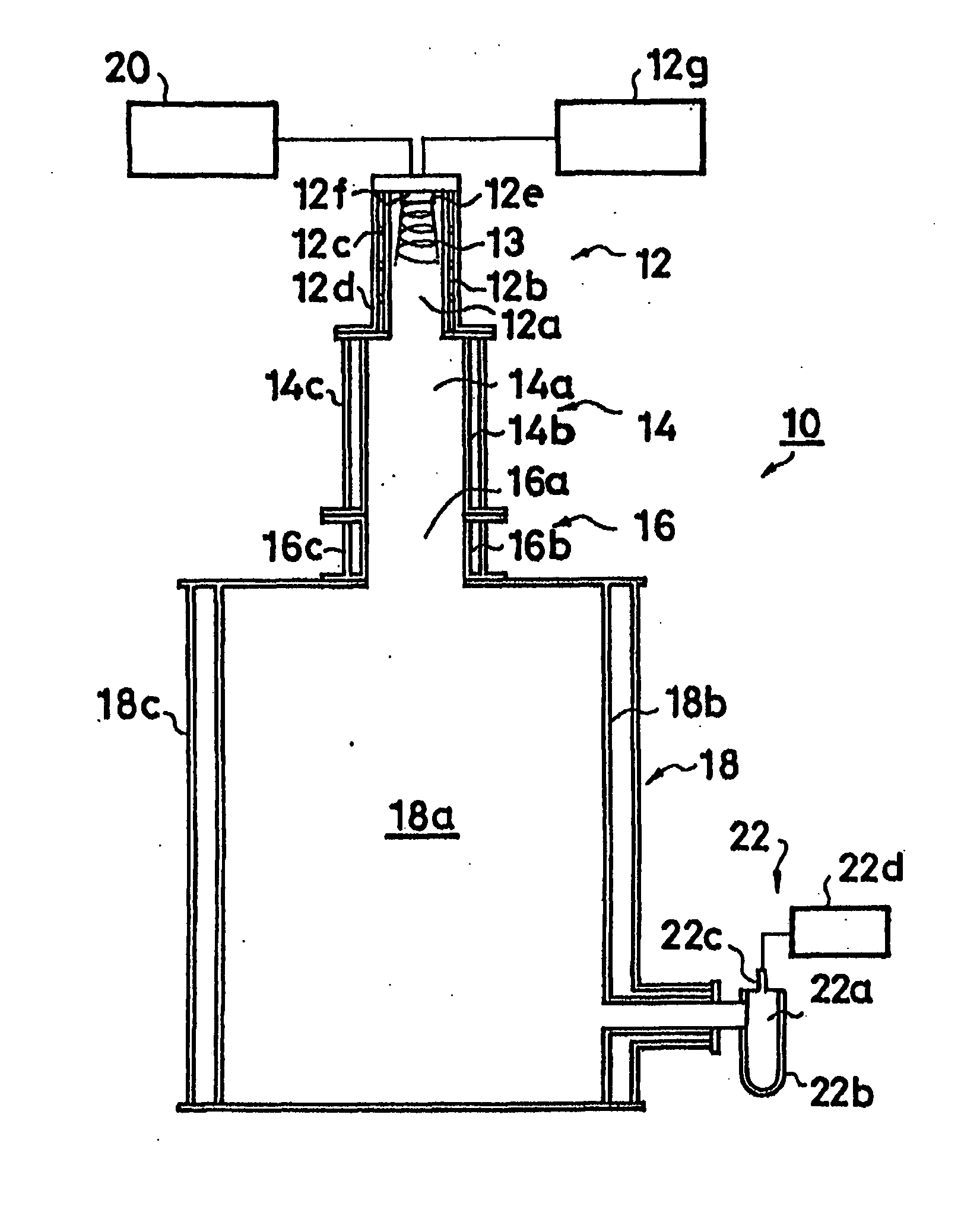
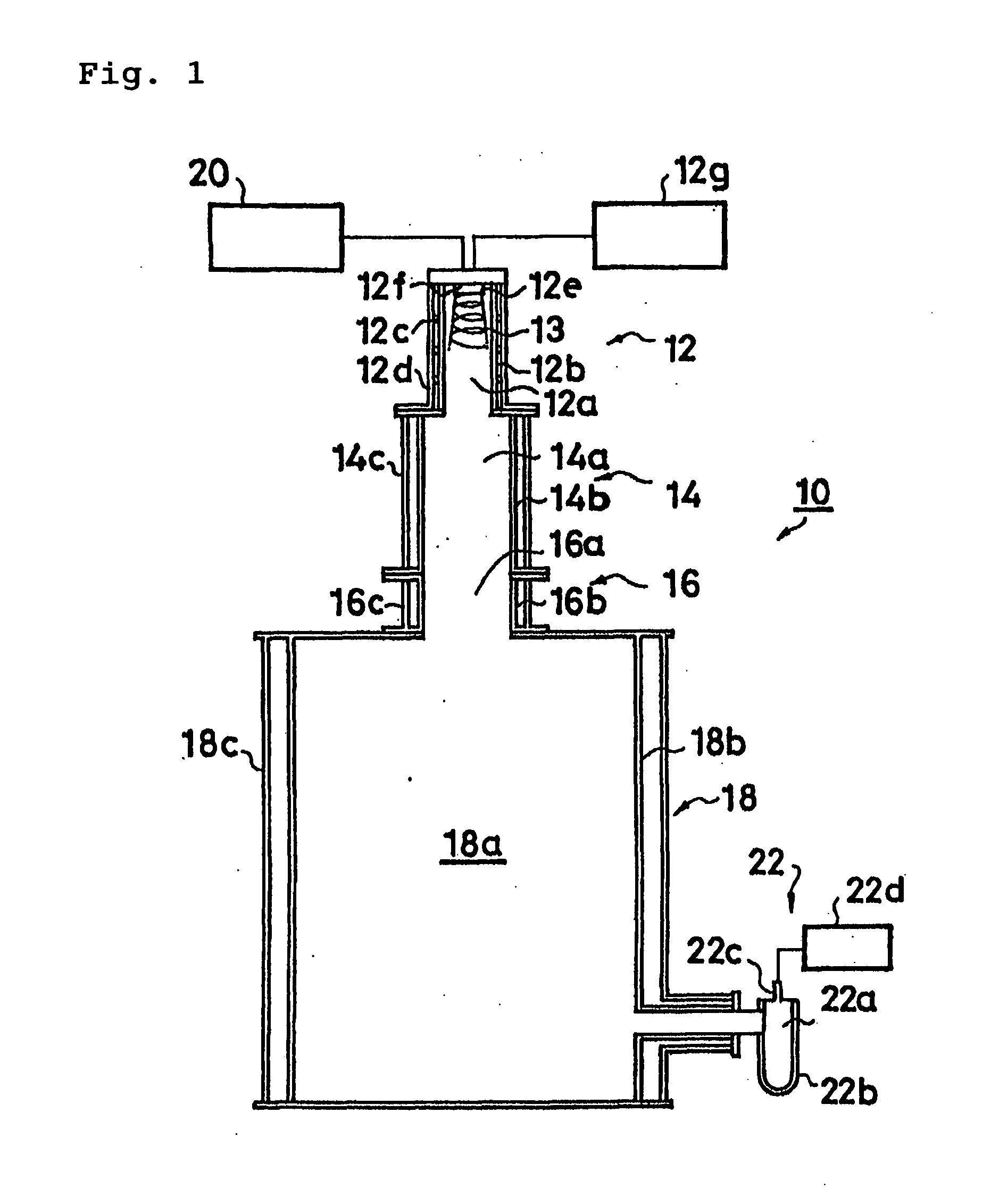
[0105] Then, silicon particles were produced by use of the thermal plasma treatment equipment 10 shown in FIG. 1. In the thermal plasma treatment equipment 10 of FIG. 1, the sizes of the quartz pipe 12b of the plasma torch 12, the quartz pipe 14b of the quartz double pipe 14, the inner pipe 16b of the cooling double pipe 16 and the inner pipe 18b of the quenching pipe 18 were 55 mm in internal diameter and 220 mm in length, 120 mm in i...

synthesis example 3

[0109] Silicon powder with an average particle diameter of 9 mm which had been obtained by dry-grinding polycrystalline silicon (resistivity: 3.3×10³ Ωcm) was further charged into a stainless steel ball mill and dry-ground in a nitrogen atmosphere at room temperature for 8 hours so as to obtain silicon fine particles having an average particle diameter of 6 μm. The thus obtained silicon fine particles having an average particle diameter of 6 μm was rinsed with 1% hydrofluoric acid and then with ion exchanged water and then vacuum-dried at 30° C.

[0110] Then, silicon particles were produced in the same manner as in Synthesis Example 2 by use of the thermal plasma treatment equipment shown in FIG. 1.

[0111] The thus produced silicon particles had an average particle diameter of 0.1 μm.


PUM

PropertyMeasurementUnit
particle diametersaaaaaaaaaa

Abstract

There are provided a silicon-film-forming composition containing silicon particles and a dispersion medium and a method for forming a silicon film by forming a coating film of the silicon-film-forming composition on a substrate and subjecting the coating film to instantaneous fusion, a heat treatment or a light treatment. According to the composition and the method, a polysilicon film with a desired thickness which may be used as a silicon film for a solar battery can be formed efficiently and easily.

Description

TECHNICAL FIELD [0001] This invention relates to a composition for forming a silicon film and a method for forming a silicon film. More specifically, the present invention relates to a silicon-film-forming composition containing specific silicon particles and a method for forming a polysilicon film by use of the composition. BACKGROUND ART [0002] As a method for forming an amorphous silicon film or polysilicon film used in production of a solar battery, a thermal CVD (Chemical Vapor Deposition) method using a monosilane or disilane gas, plasma CVD method or optical CVD method has heretofore been employed. In general, the thermal CVD method (refer to J. Vac. Sci. Technology., Vol. 14, p. 1082 (1977)) is widely used to form the polysilicon film, and the plasma CVD method (refer to Solid State Com., Vol. 17, p. 1193 (1975)) is widely used to form the amorphous silicon film. [0003] However, the formation of the silicon films by these CVD methods has problems that since a gas phase react...

Claims


Application Information

Patent Timeline
Patent Type & Authority Applications(United States)
IPC IPC(8): C23C24/10C23C26/02H01L21/208
CPCC23C24/10C23C26/02H01L21/02422H01L21/02532C30B7/005H01L21/02628H01L21/02667H01L21/02686H01L21/02601H01L21/208
Inventor MATSUKI, YASUOIWASAWA, HARUOKATO, HITOSHI
Owner JSR CORPORATIOON
Why Eureka
Try Eureka