Microstructure array, mold for forming a microstructure array, and method of fabricating the same

a microstructure array and microstructure technology, applied in the field of microstructure arrays, can solve the problems of difficult design of lenses with large na, difficult fabrication of large-area microstructure arrays, and inability to large-scale microstructure arrays, etc., to achieve convenient control of profile, reduce unusable regions, and facilitate fabrication

Inactive Publication Date: 2005-07-21
CANON KK
View PDF2 Cites 15 Cited by
  • Summary
  • Abstract
  • Description
  • Claims
  • Application Information

AI Technical Summary

Benefits of technology

[0017] It is an object of the present invention to provide a fabrication method of readily fabricating a microstructure array with reduced unusable regions between microstructures, such as microlenses, which can readily control the profile (such as the height and-the radius of curvature) of the microstructure, and fabricate the microstructure array at a relatively low cost, a fabrication method of a mold for forming a microstructure array (such as a microlens array, a fly eye lens and a lent

Problems solved by technology

In this method, however, the lens diameter cannot be large, compared with intervals between lenses.
Hence, it is difficult to design a lens with a large NA.
Further, the fabrication of a large-area microlens array is not easy, since a large scale manufacturing apparatus, such as an ion diffusion apparatus, is required to produce such a microlens array.
In addition to the above, the cost of this method is relatively high, as compared with the method using a mold.
Further, in the ion exchange method, alkaline ions for ion-exchange are indispensable in a glass substrate, and therefore, the material of the substrate is limited to alkaline glass.
The alkaline glass is, however, unfit for a semiconductor-based device which needs to be free of alkaline ions.
Furthermore, since the thermal expansion coefficient of the glass substrate greatly differs from that of a substrate of a light radiating or receiving device, misalignment between the microlens array and the devices is likely to occur due to a mismatch between their thermal expansion coefficients as the integration density of the devices increases.
Accordingly, the glass tends to warp, and hence, the difficulty in joining or bonding between the glass and the light

Method used


Image

  • Microstructure array, mold for forming a microstructure array, and method of fabricating the same
  • Microstructure array, mold for forming a microstructure array, and method of fabricating the same
  • Microstructure array, mold for forming a microstructure array, and method of fabricating the same

Examples


third embodiment

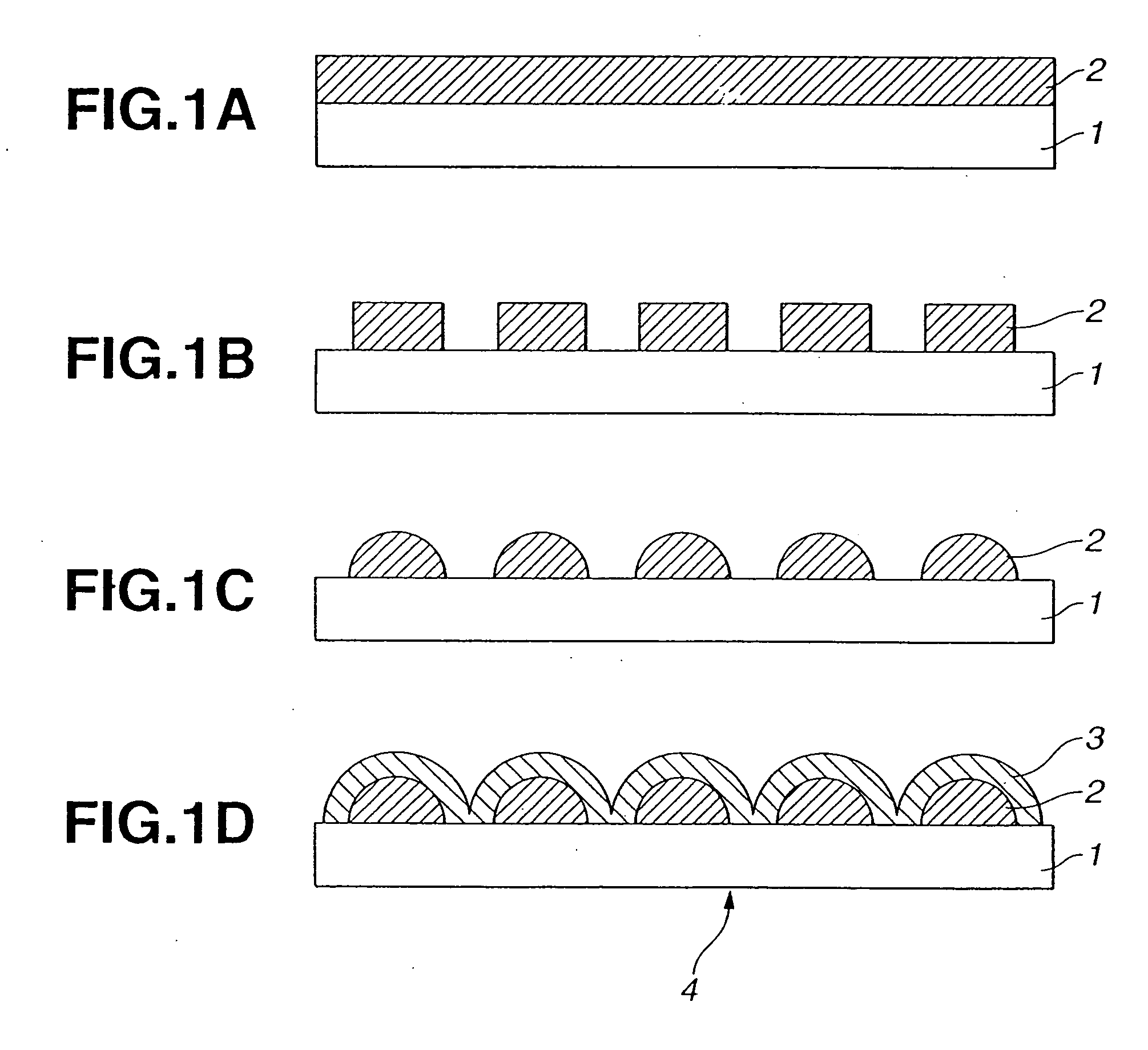
[0068] In the third embodiment, on a silicon wafer 1 with a diameter of four inches, a positive photoresist is spin-coated to a thickness of 8 μm to form a thermoplastic resin layer 2, as illustrated in FIG. 1A.

[0069] Thereafter, 1064×808 square resist microstructures 2 with sides of 16 μm are formed at common intervals of 2 μm using semiconductor photolithography, as illustrated in FIG. 1B. At the same time, a pattern for an alignment marker is formed at a desired position outside a region of the array of the resist microstructures 2.

[0070] The substrate 1 is then baked at a temperature of 150° C. for fifteen (15) minutes. The thermoplastic resin layers 2 including the pattern for the alignment marker hence undergo reflow, and spherical resin layers 2 are formed as illustrated in FIG. 1C.

[0071] Cr and Au are then continuously layered to thicknesses of 50 Å and 1000 Å on the above wafer, respectively, using an electron-beam evaporation method. An electrode layer is thus formed. Ni...

sixth embodiment

[0098] In this embodiment, a mold for a microlens array and a convex microlens array can be fabricated, in a manner similar to the The thus-fabricated microlens array also satisfies the relationship r=d / 2=12.7 μm, and each microlens has an exactly-semispherical profile.

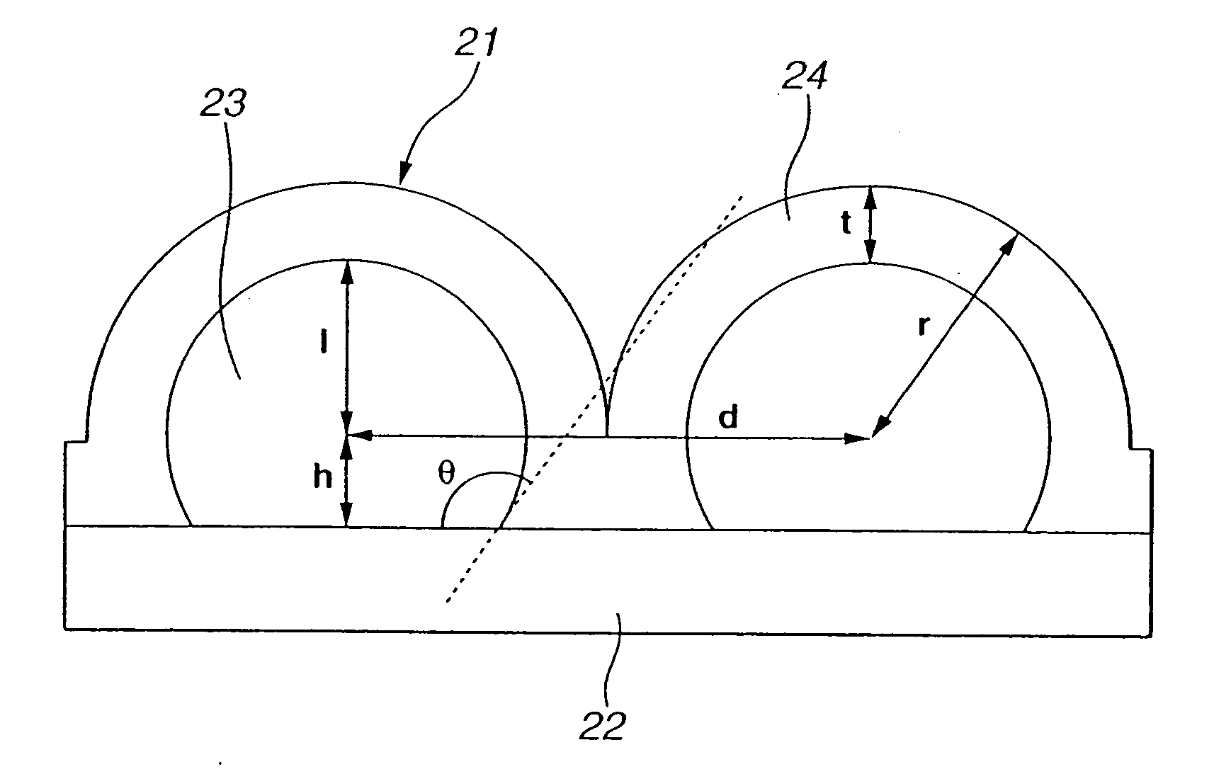
[0099] An eighth embodiment of the present invention will be described with reference to FIGS. 3, 4A, and 4C. In the eighth embodiment, on a silicon wafer 22 with a diameter of two inches, 1024×768 spherical microstructures 23 are formed at common intervals of 18 μm. An Ni electroless nickel plated layer 24 is formed on the silicon substrate 22 and the microstructures 23. The electroless plated layer 24 is a continuous layer that is isotropically grown.

[0100] In this embodiment, the radius l of the spherical microstructure 23 is 8.5 μm, the height h between the center of the spherical microstructure 23 and the substrate 22 is 4.2 μm, and the angle θ of contact between the spherical microstructure 23 and the substrat...

eleventh embodiment

[0113] the present invention will be described. In the eleventh embodiment, a quartz substrate of 24 mm×38 mm is spin-coated with a layer of polyamic acid to a thickness of 12 μm. A polyimide layer is formed by baking the wafer. A layer of aluminum (Al) is then formed by an electron-beam vacuum evaporation. A photoresist is then coated. Thereafter, 1064×808 cylindrical Al microstructures are formed at common intervals of 18 μm using semiconductor photolithography.

[0114] The polyimide layer is etched by reactive ion etching using the pattern of Al microstructures as a mask. Thus, 1064×808 cylindrical polyimide microstructures are formed at common intervals of 18 μm.

[0115] The substrate is then baked at a temperature of 450° C. for fifteen (15) minutes. The polyimide layers hence undergo reflow, and spherical layers are formed. Here, the angle of contact between the spherical resin layer and the substrate is 120 degrees. The radius l of the spherical microstructure is 8.5 μm, the hei...


PUM

PropertyMeasurementUnit
Angleaaaaaaaaaa
Microstructureaaaaaaaaaa
Areaaaaaaaaaaa

Abstract

A method for fabricating a microstructure array, such as a microlens array, and a mold for forming the microlens array, includes the steps of forming an array of microstructures with a curved profile in a discrete form on a substrate, and uniformly forming a continuous layer on the substrate and the discrete microstructures. Optically-unusable regions between the discrete microstructures, such as microlenses, can be readily reduced or eliminated by forming the continuous layer until flat portions between the microstructures disappear.

Description

BACKGROUND OF THE INVENTION [0001] 1. Field of the Invention [0002] This invention relates to a microstructure array, such as a microlens array that is usable in the field of optoelectronics and the like, a mold or a master of a mold (in the specification the term “mold” is chiefly used in the broad sense including both a mold and a master of a mold) for forming a microstructure array, a fabrication method of the microstructure array, and so forth. [0003] 2. Description of the Related Background Art [0004] A microlens array typically has a structure of arrayed minute lenses each having a diameter from about 2 to 3 microns to about 200 or 300 microns and an approximately spherical profile. The microlens array is usable in a variety of applications, such as liquid-crystal display devices, light receivers and interfiber connections in optical communication systems. [0005] Meanwhile, earnest developments have been made to develop a surface emitting laser and the like that can be readily...

Claims


Application Information

Patent Timeline
IPC IPC(8): B32B3/08C23C18/16C25D1/10G02B3/00
CPCB32B3/08C23C18/1608C23C18/1865C23C18/1893C25D1/10Y10T428/24479G02B3/0031G02B3/0056G02B3/0075Y10T428/24537Y10T428/24521G02B3/0018
Inventor TESHIMA, TAKAYUKIYAGI, TAKAYUKI
Owner CANON KK
Why Eureka
Try Eureka