

Method of forming a thick film dielectric layer in an electroluminescent laminate
a technology of electroluminescent laminate and thick film, which is applied in the direction of electroluminescent light sources, coatings, electric lighting sources, etc., can solve the problems of inability to produce bright, stable full colour, and three colours cannot all be brightly enough, so as to improve the dielectric properties reduce the porosity and the thickness of the layer, and improve the effect of the dielectric layer
- Summary
- Abstract
- Description
- Claims
- Application Information
AI Technical Summary
Benefits of technology
Problems solved by technology
Method used
Image

Examples
example 1
Isostatically Pressed Thick Film Dielectric Layer
[0178] A first layer of Heraeus CL90-7239 (Heraeus Cermalloy, Conshohocken, Pa.) high dielectric constant paste was screen printed using a 250 mesh screen having a 1.6 μm wire diameter. The high dielectric constant material in the paste was PMN-PT. The printed paste was dried for between 30 and 60 minutes at 150° C., with the longer times for a more heavily loaded oven. A second layer of the same material was printed over the baked first layer and then baked in at 300° C. for 30 min. The thickness of the combined layers at this point was about 26 μm. The entire structure was next cold isostatically pressed (CIPped) using a cold isostatic press at 350,000 kPa (50,000 psi). To ensure adequate pressing and to develop a relatively smooth surface on the dielectric layer, a sheet of aluminized polyester, with the aluminized surface in contact with the dielectric, was laid over the dielectric surface. A further two sheets of plastic bagging...
example 2
Two Layer Patterned Phosphor Structure
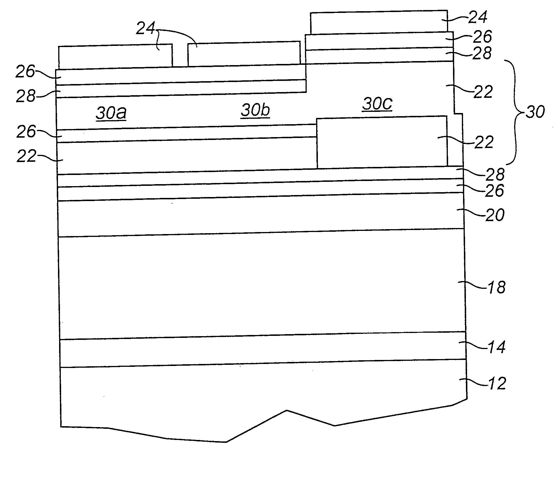
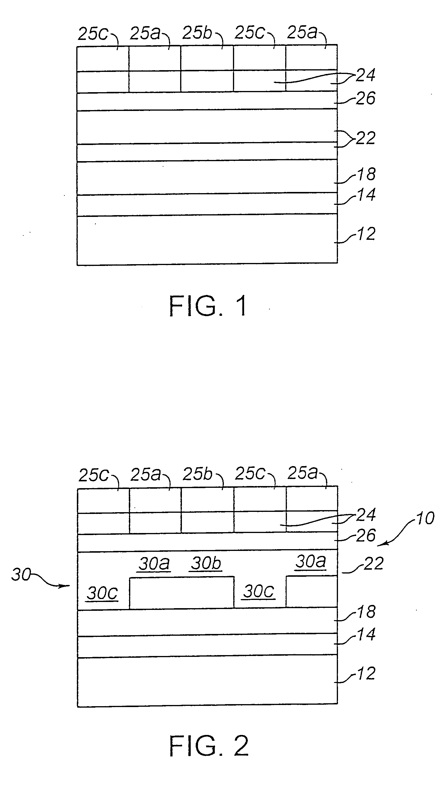
[0182] Reference may be had to FIG. 6 for the EL laminate of this example.
2.1. Thick Film Substrate Layers
[0183] The purpose of the thick film substrate is to provide a mechanical support, a first pixel electrode, and a thick film dielectric layer to electrically isolate the electrode from the phosphor structure. The electrical isolation is required to provide a means to control the density of current over a large area of pixels. The current control results from the injection of localized charge into the phosphor structure from the vicinity of the interface between the phosphor and a dielectric material in contact with it, rather than from the electrode itself. The dielectric layer has a high dielectric constant to minimize the voltage drop across it when a voltage is applied between the pixel electrodes, and a dielectric strength sufficient to prevent an electric breakdown of the dielectric when an appropriate voltage is applied between the...
example 3
Single Layer Phosphor Structure
[0207] This variant of the patterned phosphor structure requires only a single SrS:Ce deposition and includes in the same layer, a manganese doped zinc magnesium sulfide for the red and green sub-pixel elements. For Zn1-xMgxS:Mn, the value of x was in the range from 0.1 to 0.3. This phosphor has a much stronger green emission than ZnS:Mn, and can provide adequate green emission without the use of a double layer structure employing SrS and ZnS phosphors. The fabrication was as follows:
3.1. Thick Film Substrate
[0208] The substrate for this example was a 1.02 mm thick alumina sheet of approximate dimensions 12×15 inches upon which a set of 480 gold conductor strips were printed using Heraeus RP 20003 / 237-22% organometallic paste obtained from Heraeus Cermalloy and fired to form the addressing rows of a VGA format 17 inch diagonal display. The center-to-center spacing of the fired gold rows was 540 μm, the width of the rows was 500 μm and the length of...
PUM
| Property | Measurement | Unit |
|---|---|---|
| thickness | aaaaa | aaaaa |
| thickness | aaaaa | aaaaa |
| thickness | aaaaa | aaaaa |
Abstract
Description
Claims
Application Information