Fluorene compound and organic light-emitting device using same

a fluorene compound and organic light-emitting technology, applied in the direction of organic semiconductor devices, solid-state devices, discharge tubes/lamp details, etc., can solve the problems of insufficient current art and many durability problems, and achieve excellent durability, low applied voltage, and high luminance

Inactive Publication Date: 2005-10-27
CANON KK
View PDF22 Cites 85 Cited by
  • Summary
  • Abstract
  • Description
  • Claims
  • Application Information

AI Technical Summary

Benefits of technology

[0024] An organic light-emitting device which uses the fluorene compound represented by the general formula [I] can emit light at a high luminance with a low applied voltage and has excellent durability. In particular, an organic layer that contains the fluorene compound according to the present invention is excellent as an electron-transporting layer and as a light-emitting layer.
[0025] In addition, the device can be prepared by using a vacuum evaporation method or a casting method, so that a device having a large area can easily be prepared at a relatively low cost.

Problems solved by technology

In addition, many problems still remain to be solved regarding durability against the change over time due to long-term use, deterioration caused by atmospheric gas containing oxygen, moisture, or the like.
Furthermore, when considering application to a full color display or similar device, the present art is still insufficient against problems relating to the needs for light emission of blue, green, and red with a high color purity.

Method used


Image

  • Fluorene compound and organic light-emitting device using same
  • Fluorene compound and organic light-emitting device using same
  • Fluorene compound and organic light-emitting device using same

Examples


synthesis example 1

[0118] [Synthesis of Exemplified Compound No. 1]

[0119] To a 500-ml three-neck flask, 2.0 g (5.68 mmol) of 2,7-dibromo-9,9-dimethylfluorene [1], 4.2 g (17.0 mmol) of pyrene-1-boronic acid [2], 120 ml of toluene, and 60 ml of ethanol were added. Then, an aqueous solution of 24 g of sodium carbonate in 120 ml of water was added dropwise therein with stirring in a nitrogen atmosphere at room temperature, followed by the addition of 0.33 g (0.28 mmol) of tetrakis (triphenylphosphine) palladium (0). After stirring the mixture for 30 minutes at room temperature, the temperature was raised to 77° C., followed by stirring for 5 hours. After the reaction, an organic layer was extracted with chloroform and then dried with anhydrous sodium sulfate, followed by purification with a silica gel column (hexane and toluene mixture developing solvent). Consequently, 3.0 g (89% yield) of a compound [3] (white crystal) was obtained.

[0120] To a 500-ml three-neck flask, 3.51 g (5.89 mmol) of compound [3...

synthesis example 2

[0121] [Synthesis of Exemplified Compound No. 14]

[0122] To a 500-ml three-neck flask, 1.50 g (2.52 mmol) of compound [3], 1.61 g (7.55 mmol) of 1-bromoadamantane and 100 ml of dichloromethane were added. The resultant mixture was stirred at 0° C., and then 0.70 g (5.30 mmol) of aluminum chloride was slowly added thereto. After stirring the mixture for 30 minutes at 0° C., the temperature was raised to room temperature, followed by stirring for 5 hours. After the reaction, an organic layer was taken into 200 ml of water, extracted with chloroform and then dried with anhydrous sodium sulfate, followed by purification with a silica gel column (hexane and toluene mixture developing solvent). Consequently, 1.42 g (65% yield) of exemplified compound No. 14 (white crystal) was obtained.

example 1

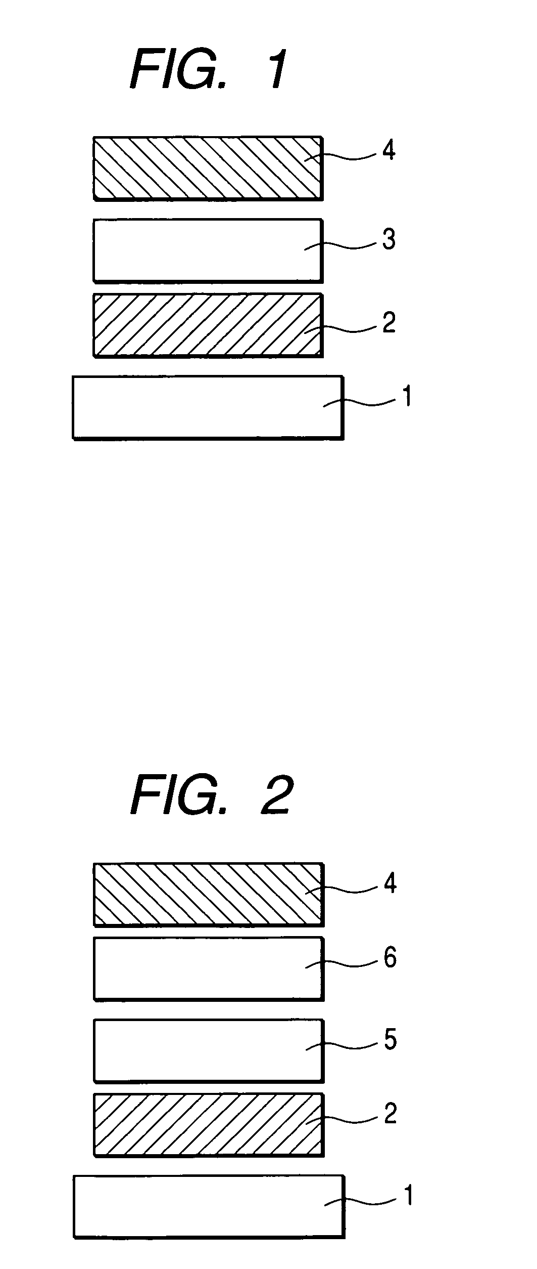
[0123] A device having the structure shown in FIG. 2 was prepared.

[0124] On a glass substrate as the substrate 1, indium tin oxide (ITO) was deposited to form a film with a thickness of 120 nm by sputtering method to obtain the anode 2, so that the substrate thus formed was used as a transparent conductive support substrate. The substrate was subjected to ultrasonic cleaning sequentially with acetone and with isopropyl alcohol (IPA). Following this, the substrate was washed with IPA through boiling and then dried. Furthermore, the substrate after UV / ozone cleaning was used as the transparent conductive support substrate.

[0125] On the transparent conductive support substrate, a chloroform solution of the compound represented by the following structural formula was applied to form a film of 30 nm in thickness by a spin-coating method, thereby forming the hole-transporting layer 5.

[0126] Furthermore, a fluorene compound represented as exemplified compound No. 1 was deposited to for...


PUM

PropertyMeasurementUnit
applied voltageaaaaaaaaaa
thicknessaaaaaaaaaa
thicknessaaaaaaaaaa

Abstract

A novel substituted fluorene compound is provided which is represented by the general formula [I]:

Description

BACKGROUND OF THE INVENTION [0001] 1. Field of the Invention [0002] The present invention relates to a novel organic compound and an organic light-emitting device using the same. [0003] 2. Related Background Art [0004] An organic light-emitting device is a device in which a thin film comprising a fluorescent organic compound or a phosphorescent organic compound is sandwiched between an anode and a cathode and electrons and holes are injected from the respective electrodes to generate excitons of the fluorescent compound or the phosphorescent compound, whereby light emitted when the excitons return to a ground state is utilized. [0005] According to a study at Kodak company in 1987 (Appl. Phys. Lett. 51, 913 (1987)), there has been reported a light emission of approximately 1000 cd / m2 at an applied voltage of approximately 10 V in a device having a function-separation type two-layer structure using ITO as an anode, a magnesium-silver alloy as a cathode, an aluminum quinolinol complex ...

Claims


Application Information

Patent Timeline
Patent Type & Authority Applications(United States)
IPC IPC(8): C07C13/465C07C13/567C07C13/66C07C211/54C07C211/61H01L51/50C07C255/49C07F7/08C09K11/06H01J1/62H01J63/04H01L51/00H05B33/14H05B33/22
CPCC07C13/567H05B33/14C09K11/06C09K2211/1011C09K2211/1014C09K2211/1029C09K2211/1033C09K2211/1037C09K2211/1048C09K2211/1059C09K2211/1088C09K2211/185C09K2211/186C09K2211/188H01L51/0039H01L51/0054H01L51/0058H01L51/0059H01L51/006H01L51/5012H01L51/5048H01L2251/308C07C211/61Y10S428/917H10K85/115H10K85/622H10K85/626H10K85/633H10K85/631H10K50/14H10K50/11H10K2102/103
Inventor YAMADA, NAOKISAITOH, AKIHITOOKINAKA, KEIJISUZUKI, KOICHISENOO, AKIHIRO
Owner CANON KK
Why Eureka
Try Eureka