Wiring board and production method thereof, and semiconductor apparatus

a technology of wiring board and production method, applied in the direction of plasma technique, printed circuit aspects, metal adhesion improvement of insulation substrates, etc., can solve the problem of requiring tens of microns of an uneven spot to ensure sufficient adhesion, and difficult to create fine wiring with a line width not exceeding tens of microns, etc. problem, to achieve the effect of easy mounting multiples

Inactive Publication Date: 2005-12-08
SAITO TOSHIRO +2
View PDF10 Cites 16 Cited by
  • Summary
  • Abstract
  • Description
  • Claims
  • Application Information

AI Technical Summary

Benefits of technology

[0014] The present invention generates amide group by modifying the surface of the resin substrate featuring excellent heat resistance and dimensional stability, and the metal having a reduction potential more base than that of copper is deposited thereon. The oxide layer of said metal is formed at the interface of the two, then copper is deposited on said metal to raise adhesion between the resin substrate and copper and to minimize degeneration of adhesion at a high temperature, thereby getting an extremely reliable wiring board. Copper wiring is formed on the resin substrate according to the full-additive method which is very effective for the formation of fine steel wire having a line width of tens of microns on said resin substrate.
[0045] A wiring layer can be laminated by repetition of a step of coating the insulating resin coating solution on the conductive wire and drying it and a step of forming the conductive wiring. The insulating layer is made flat by grinding, as required. When an insulating resin film is used as an insulating layer, conductive wiring is formed on the resin film and conductive wiring sheet is created. Another conductive wiring sheet is laminated thereon with an adequate adhesive sheet held in-between, and heat and pressure is applied, thereby completing lamination. Electric connection between layers can be easily achieved by formation of a via-hole with laser beam and by plating inside the via-hole or filling of conductive paste.
[0046] Depending on the purpose of use, the wiring board according to the present invention can be used as a flexible wiring board independently by itself, or can be used as a rigid wiring board when it is mounted on the ceramic or glass plate or silicon wafer. Furthermore, it can be used as an integral wiring board when the wiring board according to the present invention is mounted on the ceramic wiring board, and electric connection between the two is provided. Still further, wiring board according to the present invention allows easy mounting of multiple ICs on the surface; therefore, it can be used as a multi-chip module board. Especially, this is suited as a multi-chip module board where multiple ICs are mounted, since formation of fine copper wiring is ensured by full additive method.
[0050] Authors of the present invention have found out in the peel test that, similarly to the layer containing said amide group, a very strong interaction is applied between the degenerated layer formed by plasma treatment and metallic oxide film; therefore, a very powerful adhesion is ensured.
[0057] The present invention provides highly reliable wiring boards characterized by excellent adhesion between conductive metal and resin substrate, and superb heat resistance. This provides fine wiring having a required thickness with a line width of 40 μm or less.
[0058] A highly reliable multi-chip module featuring excellent heat resistance is provided by forming a laminated board through lamination of said multiple wiring boards wherein electric connection is made between layers, and a connection port with ICs is provided on the outermost surface to mount the ICs.

Problems solved by technology

When copper-made wiring is formed on the organic insulating resin substrate, the biggest problem is how to get a close adhesion between the copper wiring and resin substrate.
This method, however, requires tens of microns of an uneven spot to ensure sufficient adhesion.
It has been difficult to create fine wiring having a line width not exceeding tens of microns.
This makes it difficult to produce a fine line / space pattern.
This method is suited for the substrate with its surface having tens of microns of an uneven spot, such as the copper-plated laminate with copper etched out, but cannot be used for a more smooth substrate since effective adhesion cannot be ensured.
When ground metal and copper coexist, however, it is very difficult to etch only the ground metal.
This will raise a problem that, when the wiring board is laminated with insulating adhesive resin, this clearance is not sufficiently filled with adhesive resin, and remains as void.
Furthermore, even when ground metal other than copper is used, there is no etching process.
However, one of the big problems with the full additive method is that it is difficult to provide electroless plating to the resin substrate with excellent adhesion.
In creating a fine line pattern not exceeding 40 μm, it has been difficult to use the substrate having an uneven spot not less than microns.
However, this Official Gazette failed to provide a thick layer of one micron or more by electroless plating.

Method used


Image

  • Wiring board and production method thereof, and semiconductor apparatus
  • Wiring board and production method thereof, and semiconductor apparatus
  • Wiring board and production method thereof, and semiconductor apparatus

Examples


embodiment 1

[0071] Polyimide film resin substrate, Kapton 200H by Dupont having a surface roughness of 0.1 am or less was used. A 10 cm×10 cm sample was created, and was treated in aqueous solution for surface modification at a liquid temperature of 25° C. for 2 minutes.

[Composition of aqueous solution for surface modification]Sodium hydroxide100 g / lEthylene diamine 70 g / lEthanol100 g / l

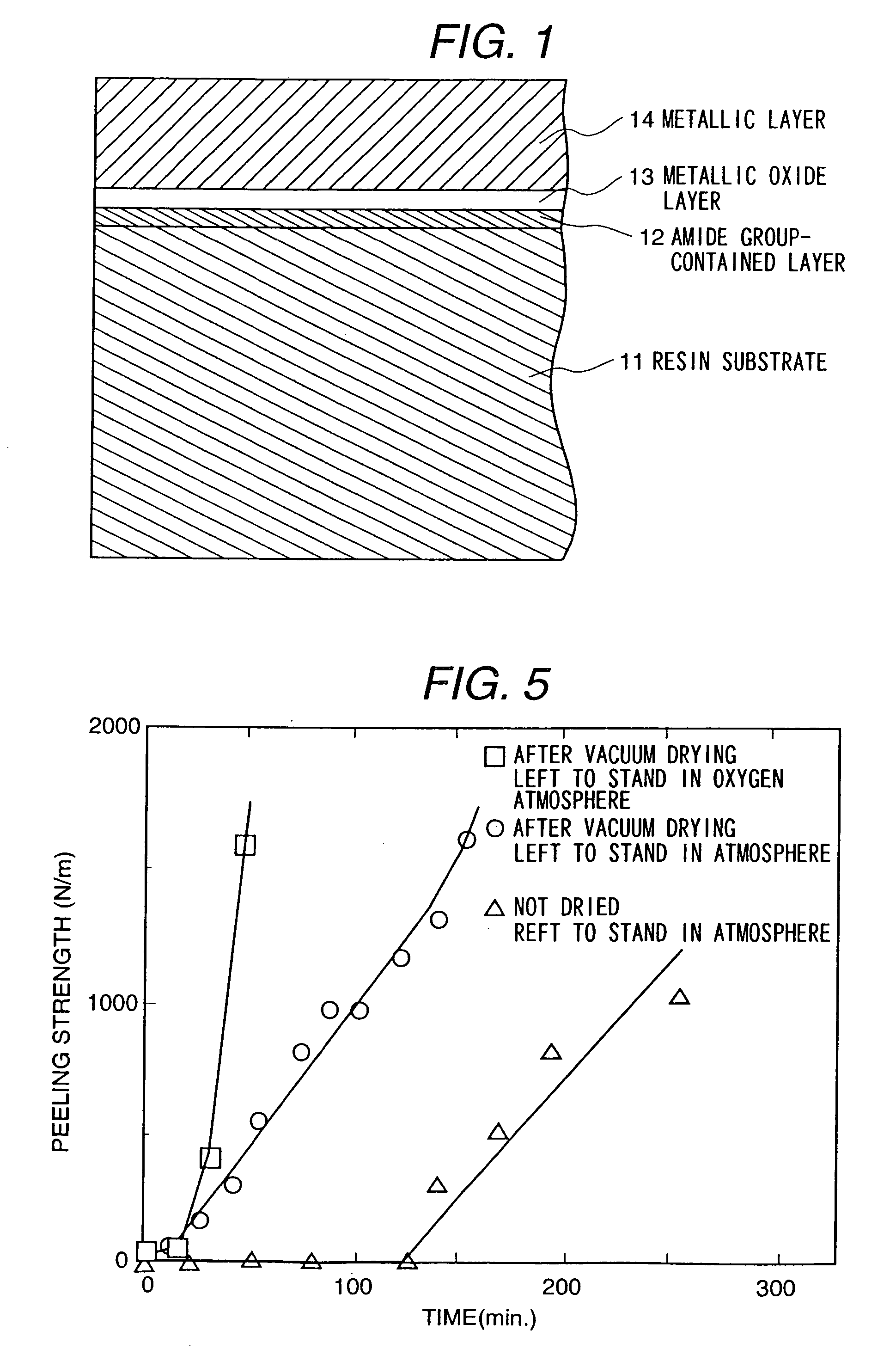
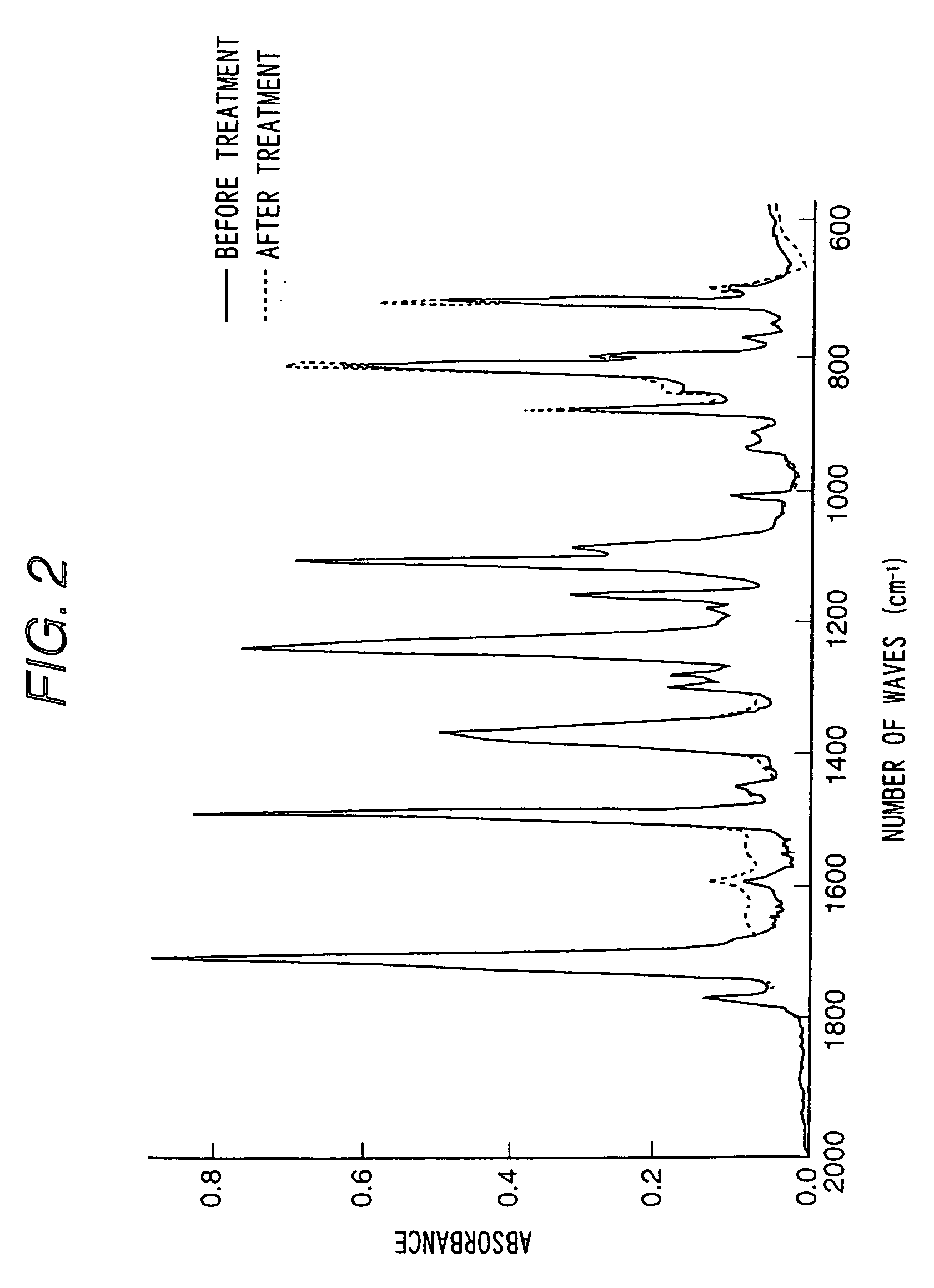
[0072] A treated sample was bonded on the epoxy resin substrate with glass cloth, and was vacuum dried at 25° C. for 3 hours. Then the sample surface was pressed against the germanium prism to measure total reflection infrared absorption. Then absorption peak specific to amide group was observed in the vicinity of 1650 cm−1 and 1550 cm−1, in addition to absorption peak in the vicinity of 1780 cm−1 and 1720 cm−1 which were attributable to the carbonyl group of the imide ring. This shows that amide group is introduced on the surface by this surface treatment. This sample was subjected to plating catalyst treatmen...

embodiment 2

[0074] Kapton 200H by Dupont was used as Polyimide film. A 10 cm×10 cm sample was created, and was treated in aqueous solution for surface modification (the same one used in the First Embodiment) at a liquid temperature of 25° C. for 2 minutes. After treatment, the sample was bonded on a glass epoxy resin substrate, and was subjected to plating catalyst treatment according to the specified method using the circuit breakers 3040, 3340 and 4041 by Japan Mining. Then electroless nickel plating solution (B-1 by Okuno Seiyaku) was used to deposit nickel to a film thickness of about 0.1 μm. After plating, the sample was separated from glass epoxy resin substrate, and was left to stand in the flow of oxygen for one hour after having been vacuum dried for three hours while kept heated to a temperature of 40° C. X-ray was irradiated from the polyimide film side at a low angle to measure diffraction spectrum and to check the interface between the polyimide film and nickel film, thereby verify...

embodiment 3

[0075] Kapton 200H by Dupont was used as Polyimide film. Four 5 cm×5 cm samples were created, and was treated in aqueous solution for surface modification (the same one used in the First Embodiment) at a liquid temperature of 25° C. for 2 minutes.

[0076] After treatment, the sample was bonded on a glass epoxy resin substrate, and was vacuum dried 25° C. for three hours. Then cobalt, tin, copper and nickel were deposited on the sample by sputtering to a thickness of about 1 μm. After that, the sample was separated from glass epoxy resin substrate, and was left to stand in the flow of oxygen for one hour. X-ray was irradiated from the polyimide film side at a low angle to measure diffraction spectrum and to check the interface between the polyimide film and metallic film, thereby verifying presence of oxides at the interface for any metal samples. Copper was then deposited on each sputtered metal film by copper electroplating to a film thickness of about 20 μm under the same condition...


PUM

PropertyMeasurementUnit
velocityaaaaaaaaaa
temperatureaaaaaaaaaa
thicknessaaaaaaaaaa

Abstract

Provided is a wiring board and production method thereof, wherein production of wiring by a full additive method is achieved. This is extremely useful in forming fine copper wiring featuring a high adhesion on an insulating resin substrate. A resin having an excellent alkali resistance is used as the insulating resin substrate, and the copper wiring is formed on the insulating resin substrate through a degenerated layer containing amide group and a metallic oxide layer of a metal having a reduction potential more base than that of copper. The degenerated layer can be provided by, e.g., introduction of amide group into the surface of the insulating resin substrate. The copper can be formed by processes including electroless plating. The insulating resin substrate has superb heat resistance and dimensional stability, and the formed structure can provide a highly packed wiring board.

Description

BACKGROUND OF THE INVENTION [0001] The present invention relates to a wiring board and production method thereof, and semiconductor apparatus made up thereof. [0002] Increasing speed and density in LSI technology in recent years have come to require a finer size of electronic circuit wires, a multi-layered structure and further improvement of electric characteristics. To meet these requirements, studies have been made to manufacture multi-layered wiring boards made up of organic insulating materials featuring excellent flatness, heat resistance, dimensional stability and dielectric characteristics. [0003] When copper-made wiring is formed on the organic insulating resin substrate, the biggest problem is how to get a close adhesion between the copper wiring and resin substrate. Conventionally, it was the common practice to improve adhesion with the metallic film deposited on the resin substrate surface through anchoring effect or mechanical entanglement by roughening the resin substr...

Claims


Application Information

Patent Timeline
Patent Type & Authority Applications(United States)
IPC IPC(8): H05K3/18H01L21/48H05H1/00H05K1/03H05K3/38H05K3/46
CPCH01L21/4846H05K3/381H05K3/389H05K3/4623H05K3/4661H05K2201/0344H05K2203/0315H05K2203/0793H05K2203/095Y10T29/49126H01L2224/16225H01L2924/00014H01L2224/0401
Inventor SAITO, TOSHIROAKAHOSHI, HARUOITABASHI, TAKEYUKI
Owner SAITO TOSHIRO
Why Eureka
Try Eureka