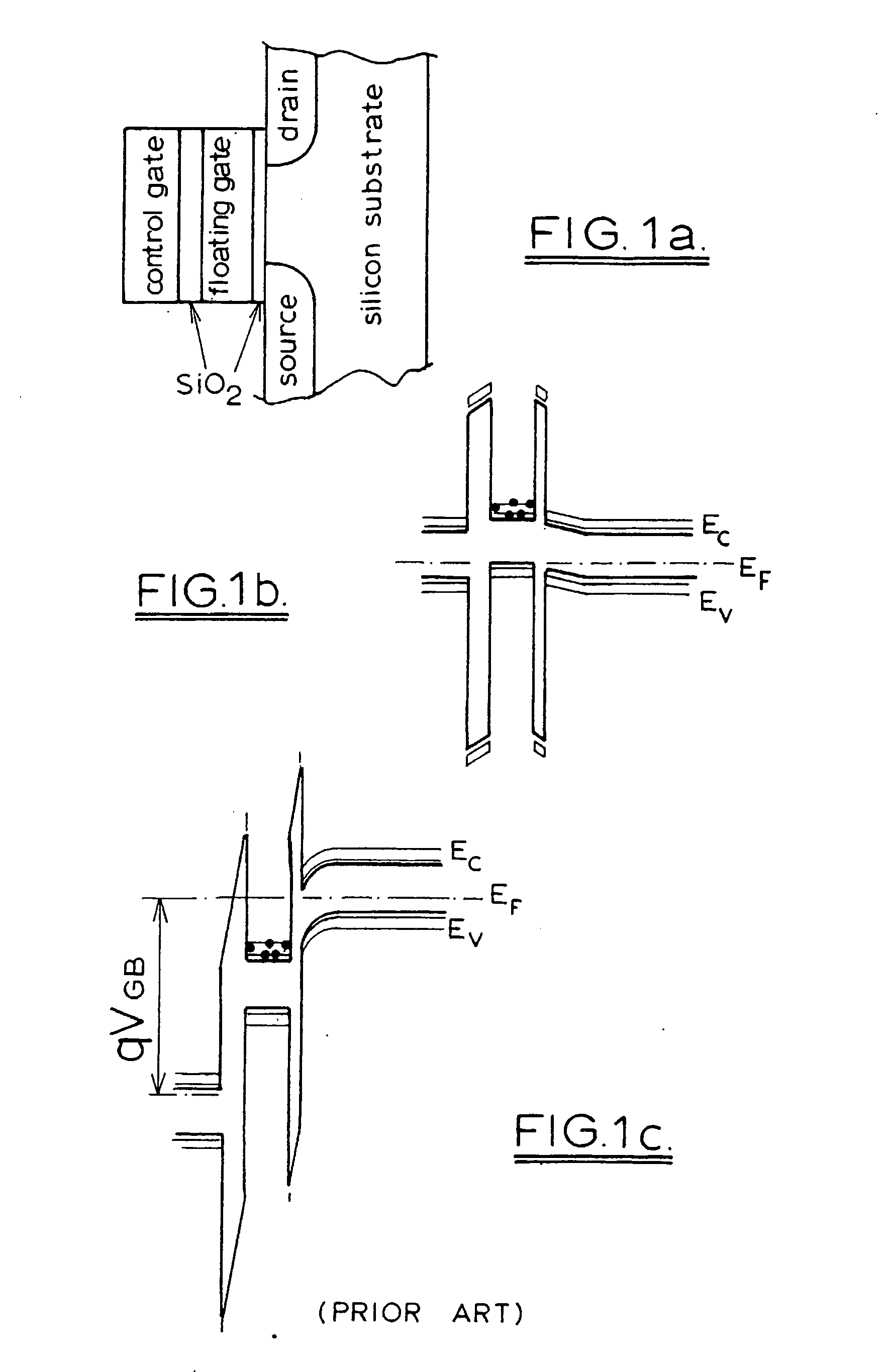
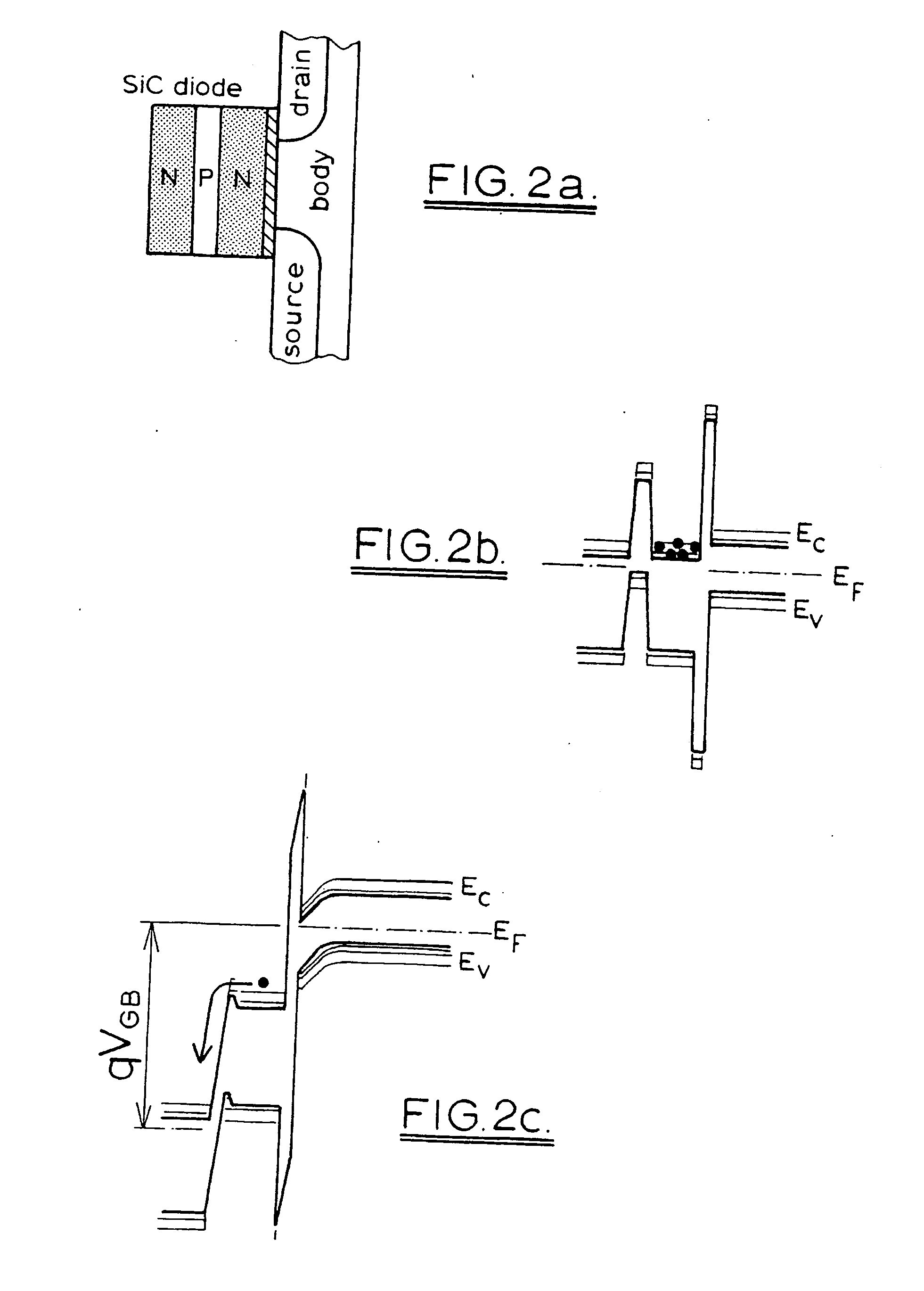
[0014] One embodiment of the invention is a modification of the 1T flash cell (prior art). The floating gate of the 1T flash cell can be considered as the connection between two
capacitor terminals—one
capacitor being between the control gate and the floating gate, and the other
capacitor being between the floating gate and the channel of the
transistor. Then, this embodiment of this invention can simply be described as a replacement of the capacitor on the control-gate side by a SiC
diode. The SiC diode can provide the
charge retention achieved by the replaced capacitor because both bulk and
surface charge generation / recombination are practically negligible in passivated SiC regions. Importantly, the SiC diode can also provide fast and nondestructive charge removal / deposition, avoiding the limitations imposed by the replaced capacitor. Designing the diode as a reference diode enables the use of both forward and reverse turn-on voltages for easier charging and discharging operations. This 1
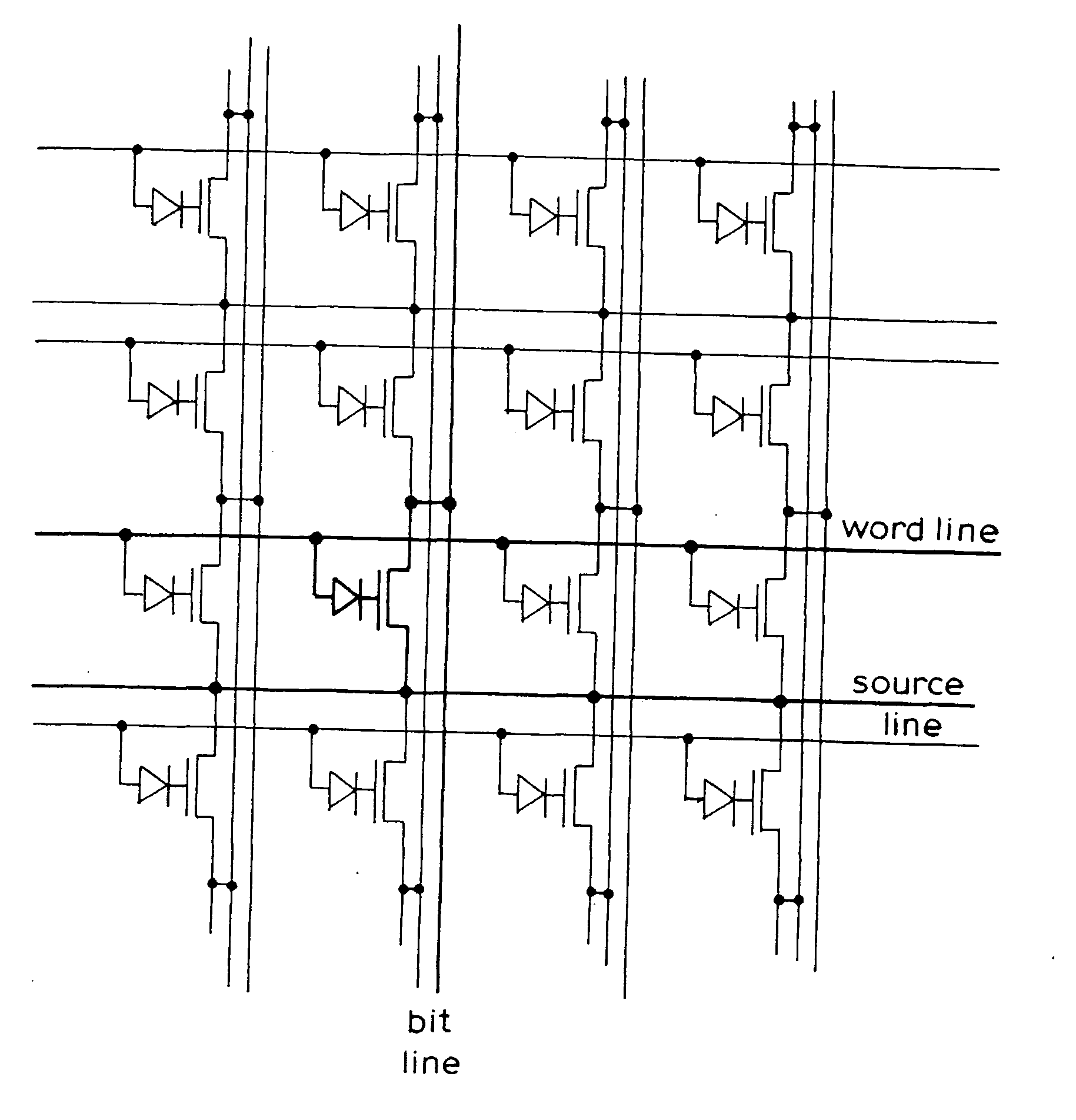
T cell with diode isolation enables straightforward implementation of the architectures used in the present flash memories, and in particular the NOR and the NAND arrays that are established as the industry standards for code and data storage.
[0017] In either embodiment, the cells are read by sensing resistance. This has the consequence of enabling multiple levels with a consequential increase in memory capacity and removes problems in
down scaling the
cell size.
[0019] Compared to Flash memory lower voltages are required and the speed of charging and discharging is greater than with Flash. The
memory cell of this invention has none of the disadvantages of Flash memory with the added benefit that the cell may have several (infinite) logic states if they are needed. Another
advantage that this invention has over Flash memory is that in Flash memory charging and discharging is destructive and changes the material state whereas in this invention the passivated interface provides fast and nondestructive charge removal / deposition. In this invention the charging and discharging of the gates through the diode does does not change the electrical properties of the material forming the diode and does not in any way stress the
gate oxide. With the dynamic memory cell of this invention the number of writing cycles is sufficiently high and the speed of discharging / charging is sufficiently quick to allow for
real time data processing. The
passivation of the Sic-SiO2 interface creates
charge retention times sufficiently long to avoid the need for the memory cell of this invention to be electrically refreshed as is the case with conventional RAM.
Charge retention times beyond 7 years are achievable with this invention.
Passivation may be by Thermal SiO2
passivation or preferably by
nitriding the surface at high temperatures with NO or N2O.
[0021] The fabrication method which results in a self aligned
MOSFET with a
metal gate provides performance improvements (better
down scaling of F, reduced
power consumption, and reduced leakage through the
gate oxide). Self-aligned MOSFETs are routinely made in silicon (either with polysilicon or
metal gates). The challenge in SiC is due to the need for high-temperature annealing to activate the
doping of the drain and the source areas after creating them by
ion implantation with the
MOSFET gates as self-aligning masks. The
ion implantation may be performed at
room temperature, but this requires prohibitively high annealing temperatures (>1400° C.). An alternative method is to perform the ion-implantation at high temperatures (about 800° C.), in which case the post
implant annealing temperature up to 1300° C. is sufficient. The challenge with this is to find a
metal (or a metal-based structure) that will provide the necessary adhesion to the
gate oxide and that will withstand the high-temperature
ion implantation. A preferred metal is
Molybdenum and this allows a Mo-gate process that satisfies the conditions for fabrication of self-aligned SiC MOSFETs by hot
ion implantation. Other suitable materials are P+ polysilicon, and
platinum silicide. An essential feature of this preferred method is the use of a capping
dielectric (deposited
oxide, for example) to prevent sublimation of the Mo gate, as well as
coating the capping
dielectric by a
thin metal film to avoid damaging charging effects during the
ion implantation.
[0040] All these advantages help to achieve higher memory capacities, as evidenced by the fact that higher memory capacities are achieved by modern flash than by modern DRAMs.

