Photoelectric conversion element and process for fabricating the same, electronic device and process for fabricating the same

a technology of photoelectric conversion and conversion element, which is applied in the direction of sustainable manufacturing/processing, final product manufacturing, electrochemical generators, etc., can solve the problems of only a small adverse effect on the global environment, a large risk of radioactive ray contamination of atomic energy, and the dependence on these kinds of energy is undesirable, so as to enhance the adhesiveness and flexibility of the semiconductor electrode, and enhance the durability of the semiconductor electrode

Inactive Publication Date: 2006-05-25
SONY CORP
View PDF25 Cites 42 Cited by
  • Summary
  • Abstract
  • Description
  • Claims
  • Application Information

AI Technical Summary

Benefits of technology

[0063] According to the invention having the above construction, it forms the semiconductor electrode by pressing the paste containing the binder and semiconductor nanoparticles dispersed therein while heating it to a temperature in the range from 30° C. to the softening temperature of the transparent conductive substrate or the substrate, or to a temperature in the range from 30° C. to the lower one of the softening temperature of the transparent conductive substrate or the substrate and the deactivation temperature of the sensitizing dye, and thereby bonding the semiconductor nanoparticles onto the substrate. Therefore, the invention can enhance the adhesiveness and flexibility of the semiconductor electrode to the substrate, and can enhance the durability of the semiconductor electrode against curving and bending.

Problems solved by technology

The use of atomic energy is accompanied by the risk of contamination by radioactive rays.
Currently under various discussions on the environmental issues, dependence upon these kinds of energy is undesirable.
On the other hand, solar cells, which are photoelectric conversion devices for converting sunlight to electric energy, use sunlight as their energy resources, and they produce only a small adverse effect to the global environment.
However, since crystalline silicon solar cells need much energy and time for crystal growth, they are disadvantageous from the viewpoint of their costs.
However, photoelectric conversion efficiency of amorphous silicon solar cells is lower than that of crystalline silicon solar cells.
Furthermore, although amorphous silicon solar cells are higher in productivity than crystalline silicon solar cells, they need an evacuation process for the manufacture.
Therefore, the burden related to facilities for fabrication of crystalline silicon solar cells is still heavy.
However, they exhibit as low photoelectric conversion coefficient as 1%, and involve difficulties in durability.
This solar cell, however, requires the use of a substrate resistible to the baking temperature as high as approximately 500° C. in the high-temperature burning process for making its porous semiconductor electrode, and here is the problem of reducing the selectable range of substrates.
However, semiconductor electrodes made by these methods are not sufficient in durability, and photoelectric conversion efficiency of solar cells currently remains lower than several %.
However, the photoelectric conversion efficiency is still lower than that of a solar cell having a semiconductor electrode made by the baking process.
In addition, although this method of making the semiconductor electrode at room temperatures makes it possible to use even a plastic substrate having low heat resistance as a support member of a transparent electrode, the semiconductor nanoparticle layer formed on the plastic substrate by pressure bonding is low in adhesiveness to the substrate and flexibility, and therefore unreliable in durability against bending or expansion and contraction.
In addition, since ethyl cellulose used in Literature 2 as a binding agent is soluble to alcohol and organic solvents, it dissolves into the dye solution and electrolytic solution used for the dying with the dye, and invites serious characteristic deterioration with time.

Method used


Image

  • Photoelectric conversion element and process for fabricating the same, electronic device and process for fabricating the same
  • Photoelectric conversion element and process for fabricating the same, electronic device and process for fabricating the same
  • Photoelectric conversion element and process for fabricating the same, electronic device and process for fabricating the same

Examples


example 1

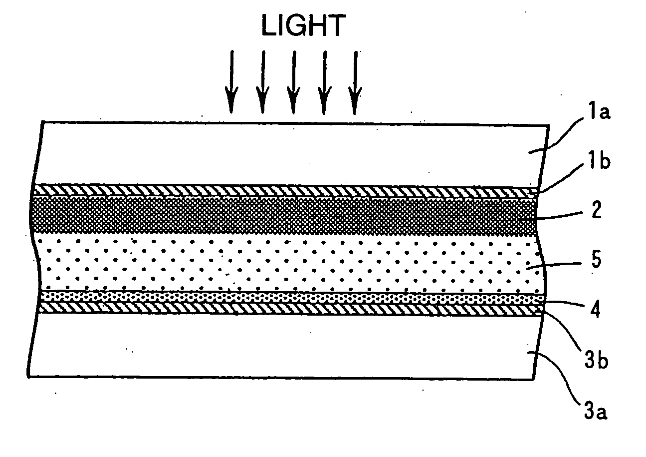
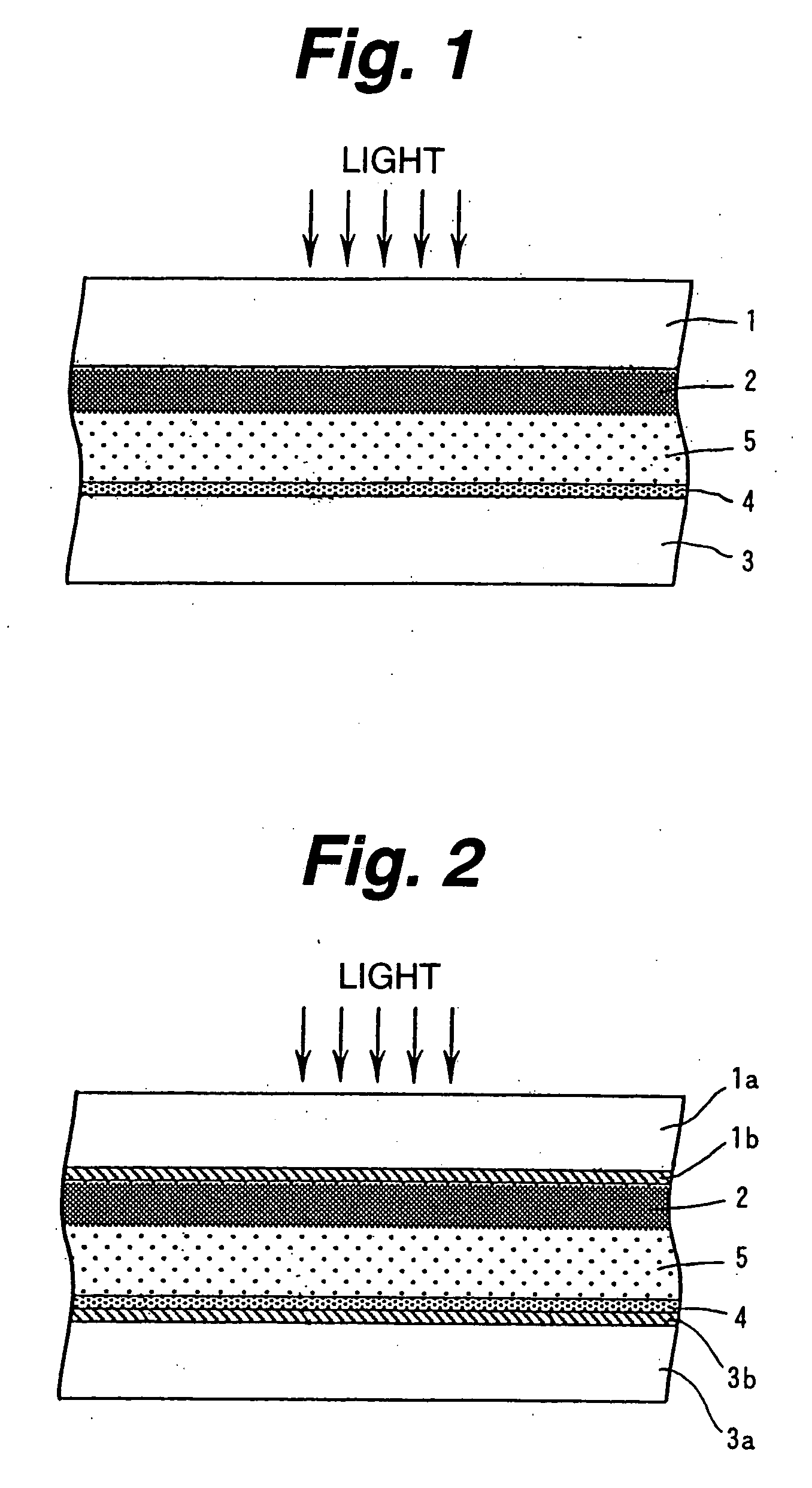
[0081] TiO2 nanoparticles were used as semiconductor nanoparticles. Referring to known methods (H. Arakawa, “Latest Techniques of Dye-sensitized Solar Cells” (C.M.C.) p. 45-47 (2001)), paste with dispersed nanoparticles was prepared as follows. 125 ml of titanium isopropoxide was seeped slowly into 750 ml of 0.1M nitric acid water solution while stirring it at the room temperature. After the seeping, the solution was moved to a constant temperature bath held° at 80° C. and stirred therein for 8 hours. Thereby, a cloudy, semi-transparent sol solution was obtained. The sol solution was left to cool down to the room temperature, then filtered through a glass filter, and 700 ml thereof was measured up. The sol solution obtained was moved to an autoclave, then treated by water and heat at 220° C. for 12 hours, and thereafter dispersed by ultrasonic treatment for one hour. Subsequently, the solution was condensed by an evaporator at 40° C. until the content of TiO2 becomes 20 wt %. The co...

examples 2 to 6

[0088] Dye sensitized wet-type photoelectric conversion devices were prepared in the same manner as Example 1 except the pressing of the paste under the conditions shown in Table 1.

example 7

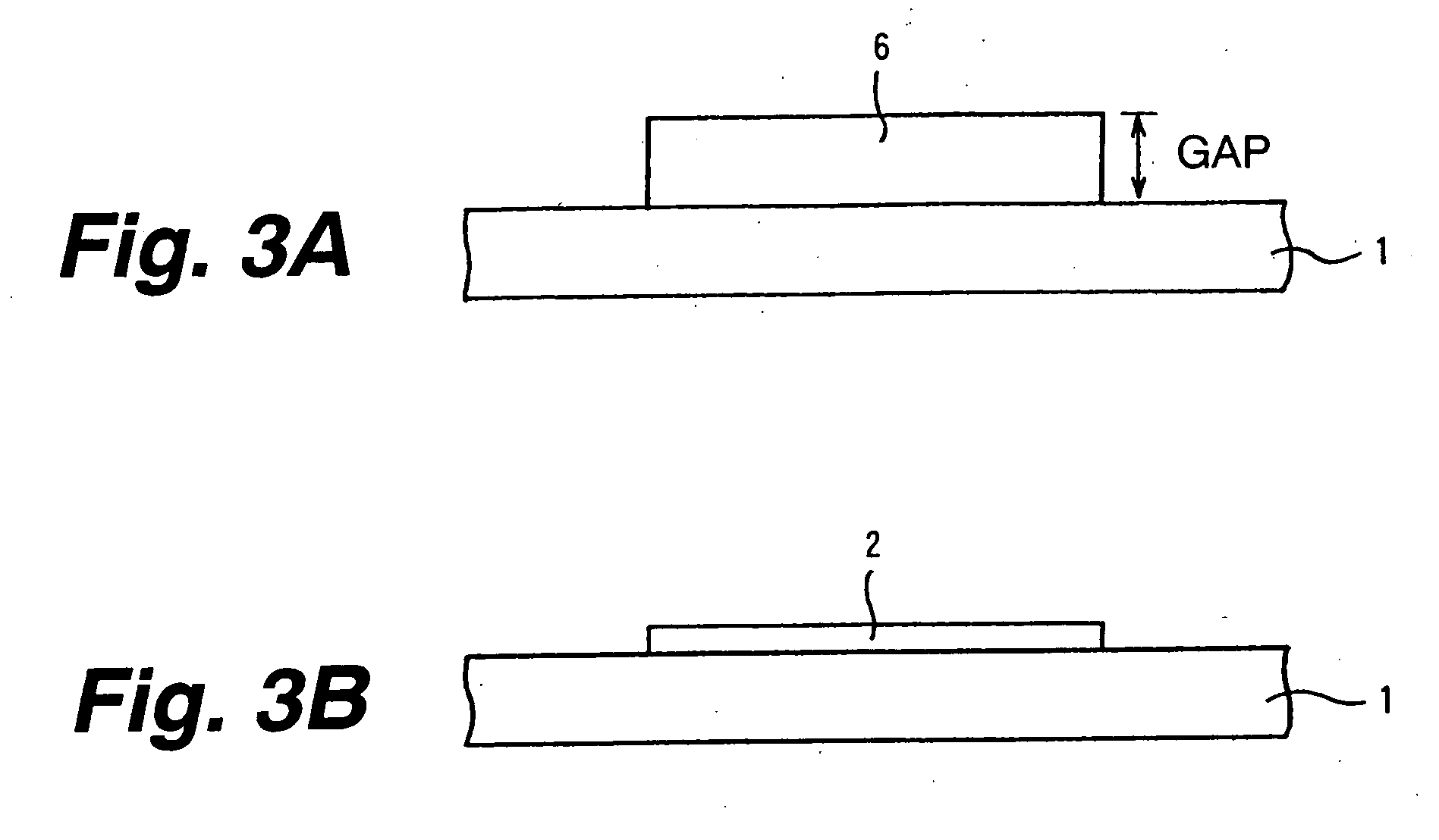
[0089] TiO2 paste prepared in the same manner as that of Example 1 was directly coated on a conductive PET substrate (having sheet resistance of 50 Ω / □) having SnO2 coating on its surface to be sized 1 cm×1 cm and make the gap of 200 μm by blade coating, and pressure of 10000 kg / cm2 was applied too the paste for 30 seconds at 120° C. by a press machine. On the dye-retained TiO2 paste nanoparticle layer thus obtained, the same dye-retained TiO2 paste was coated by another gap of 200 μm by blade coating to make a pressure-bonded dye-retained TiO2 nanoparticle layer under the same conditions.

[0090] After that, the substrate was immersed in a dehydrated ethanol solution in which 0.5 mM of cis-bis(isothiocyanate)-N,N-bis(2,2′-dipyridile)-4,4′-dicarboxylic acid)-ruthenium (II) dihydrate and 20 mM of deoxycholic acid for 12 hours to have the dye retained by the TiO2 nanoparticle layer. The dye-retained TiO2 nanoparticle layer obtained was washed first by ethanol solution of 4-tert-butyl p...


PUM

PropertyMeasurementUnit
softening temperatureaaaaaaaaaa
temperatureaaaaaaaaaa

Abstract

In a photoelectric conversion device using a semiconductor electrode composed of semiconductor nanoparticles, the semiconductor electrode is made by coating and drying a paste containing a binder and semiconductor nanoparticles dispersed therein on a transparent conductive substrate, and pressing the paste to bond the semiconductor nanoparticles onto the transparent conductive substrate while heating it to a temperature in the range from 30° C. to the softening temperature of the transparent conductive substrate, or, if the semiconductor nanoparticles retain a sensitizing dye, to a temperature in the range from 30° C. to lower one of the softening temperature of the transparent conductive substrate and the deactivation temperature of the sensitizing dye.

Description

TECHNICAL FIELD [0001] This invention relates to a photoelectric conversion device, a manufacturing method thereof, an electronic apparatus and a manufacturing method thereof, which are suitable for application to wet solar cells using semiconductor electrodes made of semiconductor nanoparticles. BACKGROUND ART [0002] It is generally recognized that the use of fossil fuel such as coal and petroleum as energy sources invites global warming by resultant carbon dioxide. The use of atomic energy is accompanied by the risk of contamination by radioactive rays. Currently under various discussions on the environmental issues, dependence upon these kinds of energy is undesirable. [0003] On the other hand, solar cells, which are photoelectric conversion devices for converting sunlight to electric energy, use sunlight as their energy resources, and they produce only a small adverse effect to the global environment. Therefore, wider promulgation of solar cells is anticipated. [0004] Although t...

Claims


Application Information

Patent Timeline
Patent Type & Authority Applications(United States)
IPC IPC(8): H01L25/00H01L31/00H01L21/288H01G9/20H01L21/208H01L21/368H01L31/0224H01L31/04H01M14/00
CPCH01G9/2031H01G9/2068H01L31/022425H01M14/005Y02E10/542Y02P70/50
Inventor MOROOKA, MASAHIROSUZUKI, YUSUKENODA, KAZUHIRO
Owner SONY CORP
Why Eureka
Try Eureka