Semiconductor device and manufacturing method thereof

a semiconductor and manufacturing method technology, applied in the direction of semiconductor devices, electrical appliances, transistors, etc., can solve the problem that single-crystal silicon film cannot easily absorb laser beams, and achieve the effect of short-channel

Inactive Publication Date: 2006-06-08
SEMICON ENERGY LAB CO LTD
View PDF11 Cites 29 Cited by
  • Summary
  • Abstract
  • Description
  • Claims
  • Application Information

AI Technical Summary

Benefits of technology

[0027] With the above structure, a semiconductor device in which leak current between a source region and a drain region due to a short-channel effect is decreased can be manufactured.
[0028] According to the present invention, since high-temperature heat can ...

Problems solved by technology

In other words, when a laser beam having this wavelength range is delivered, the extension region ...

Method used


Image

  • Semiconductor device and manufacturing method thereof
  • Semiconductor device and manufacturing method thereof
  • Semiconductor device and manufacturing method thereof

Examples


embodiment 1

[0062] Embodiment 1 will describe an example of a laser irradiation apparatus used in the present invention with reference to the drawings.

[0063] A laser oscillator 401 shown in FIG. 4 is a laser oscillator having a pulse width on a femtosecond time scale (1 femtosecond=10−15 second). This laser is also referred to as a femtosecond laser. A laser beam emitted from the laser oscillator 401 is converted into a harmonic with a wavelength of 370 to 640 nm, preferably 400 to 540 nm, by using a non-linear optical element as necessary.

[0064] As a laser used in the present invention, for example, a laser in which a crystal of sapphire, YAG, ceramic YAG, ceramic Y2O3, KGW, KYW, Mg2SiO4, YLF, YVO4, GdVO4, or the like is doped with Nd, Yb, Cr, Ti, Ho, Er, or the like is given. However, another laser which can satisfy the above condition of the pulse width and the wavelength can be used. Moreover, it is preferable to use a laser having a repetition rate of more than 10 MHz in addition to the ...

embodiment 2

[0077] Embodiment 2 will describe a procedure for manufacturing an FET which is different from Embodiment Mode.

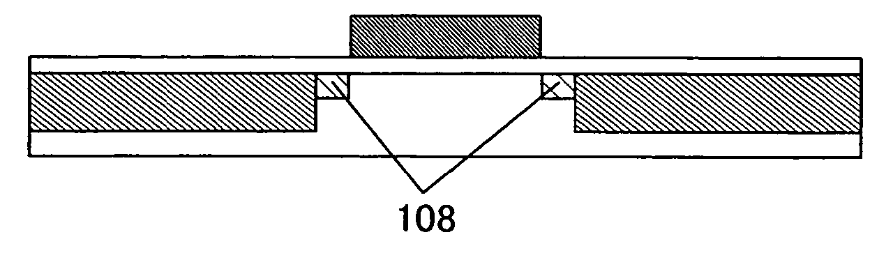
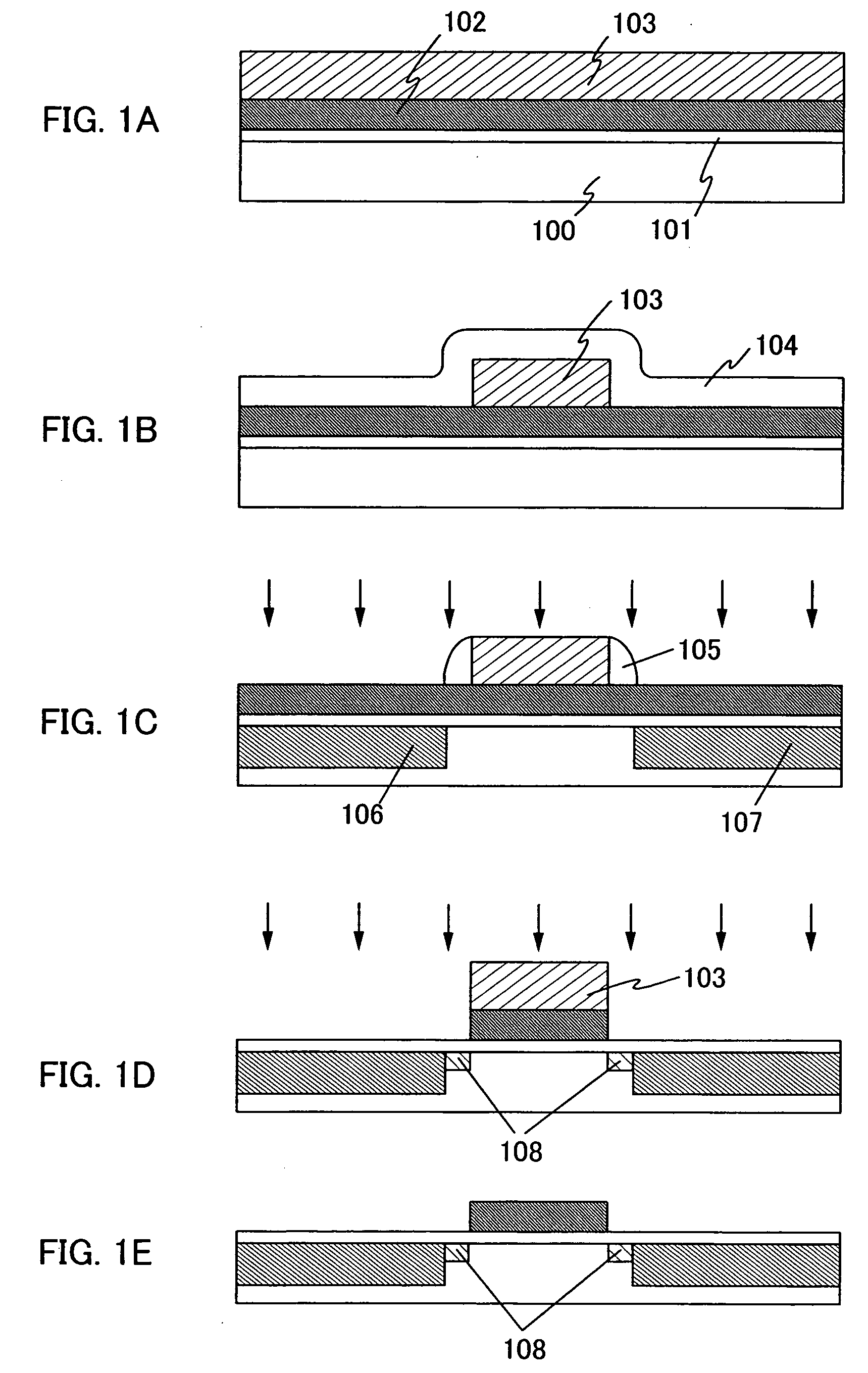
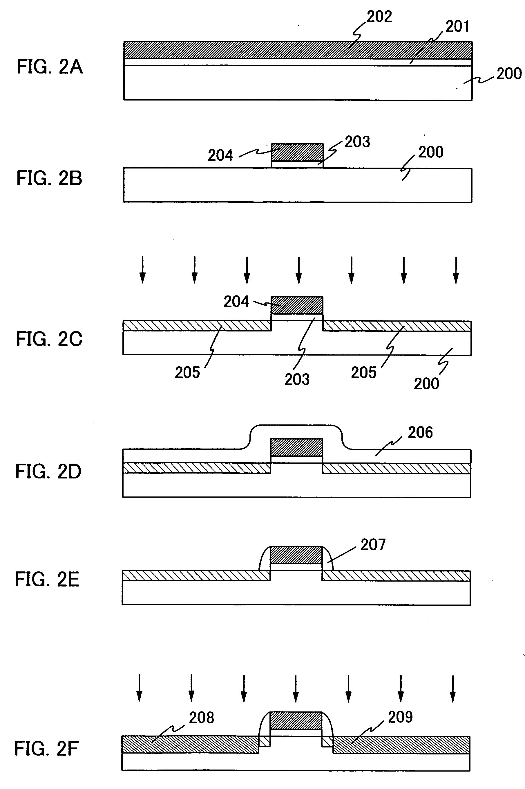
[0078] First, similarly to FIG. 1A, a gate insulating film 501, a conductive film 502, and a film 503 are formed over a single-crystal semiconductor substrate 500.

[0079] The single-crystal semiconductor substrate 500 may be, for example, an SOI (Silicon On Insulator) substrate manufactured by a pasting method or a SIMOX (Separation by IMplanted Oxygen) method or a silicon wafer. When a semiconductor element is manufactured by using an SOI substrate, the adjacent elements can be separated completely, thereby preventing the flowing of leak current.

[0080] In this embodiment, an oxide film formed by thermally oxidizing the single-crystal semiconductor substrate 500 is used as the gate insulating film 501. The gate insulating film 501 may be formed not only by a thermal oxide method used in this embodiment but also by a plasma CVD method or a sputtering method.

[0081] The for...

embodiment 3

[0105] Embodiment 3 will describe a method for manufacturing a semiconductor element with reference to FIGS. 6A to 8C. Specifically, Embodiment 3 will show an example of manufacturing a CMOS-type IC using a single-crystal silicon substrate.

[0106] First, a substrate 600 made of single-crystal silicon is prepared, and a first element forming region 602 and a second element forming region 603 are formed by a known LOCOS method or shallow trench isolation (STI) method.

[0107] Specifically, a silicon nitride film 601 is deposited onto the single-crystal silicon substrate 600, and then the silicon nitride film 601 is removed while remaining a portion thereof which will become an active region (FIG. 6A).

[0108] Then, the silicon nitride film 602 is used as a mask to form a thick silicon oxide film (field oxide film) 604 for separation by a thermal oxidation method. Next, the first element region 602 and the second element region 603 separated by the field oxide film 604 are formed by remo...


PUM


Abstract

It is an object of the present invention to provide a semiconductor device superior in the decrease in leak current due to a short-channel effect and a manufacturing method thereof. In a process of forming a field-effect transistor over a single-crystal semiconductor substrate, an impurity is introduced to form an extension region and a single crystal lattice is broken to make the extension region amorphous. Alternatively, the impurity and an element having large mass number are introduced to break the single crystal lattice and make the extension region amorphous. Then, a laser beam with a pulse width of 1 fs to 10 ps and a wavelength of 370 to 640 nm is delivered to selectively activate the amorphous portion, so that the extension region is formed with a thickness of 20 nm or less.

Description

BACKGROUND OF THE INVENTION [0001] 1. Field of the Invention [0002] The present invention relates to a method for manufacturing a semiconductor device using a laser irradiation apparatus for irradiating an object with a laser beam. Specifically, the present invention relates to a semiconductor device including a thin film transistor (hereinafter referred to as a TFT) having ultrashallow junction. For example, the present invention relates to a large scale integrated circuit (LSI), an electro-optic device typified by a liquid crystal display panel, a light-emitting display device having a light-emitting element, a light-receiving device having a CCD (charge-coupled device), a memory device such as an SRAM or a DRAM, and an electronic appliance equipped with any one of these devices as its component. [0003] In this specification, the semiconductor device indicates general devices which can function by using a semiconductor characteristic. An electro-optic device, a semiconductor circu...

Claims


Application Information

Patent Timeline
IPC IPC(8): H01L21/336
CPCH01L21/2236H01L21/268H01L21/823814H01L29/4958H01L29/511H01L29/6653H01L29/6659
Inventor TANAKA, KOICHIRO
Owner SEMICON ENERGY LAB CO LTD
Why Eureka
Try Eureka