Single crystal GaN substrate, method of growing single crystal GaN and method of producing single crystal GaN substrate

a technology of single crystal gan and substrate, which is applied in the direction of crystal growth process, polycrystalline material growth, chemically reactive gas growth, etc., can solve the problems of poor symmetry, sapphire is deprived of cleavage plane, gan films or ingan films grown on a sapphire substrate are annoyed by large lattice misfitting, etc., to achieve large volume, eliminate hazy dislocation diffusion, and large dislocation capacity

Inactive Publication Date: 2006-09-28
SUMITOMO ELECTRIC IND LTD
View PDF7 Cites 203 Cited by
  • Summary
  • Abstract
  • Description
  • Claims
  • Application Information

AI Technical Summary

Benefits of technology

[0100] Unlike a narrow defect assembly 15 as shown in FIG. 3(1), the present invention prepares wide voluminous defect accumulating regions (H) and storing dislocations by the voluminous defect accumulating regions (H) with a definite thickness. Wideness and voluminousness enable the voluminous defect accumulating regions (H) to accommodate far more dislocations than the lean defect assembly 15 of FIG. 3(1). One advantage of the present invention is the vast capacity of the voluminous defect accumulating regions (H).
[0101] Instead of polygonal pits, the present invention employ linear facets aligning as wide strips extending in a definite direction. Six radial corner lines, which accompany polygonal pits, do not occur on a surface composed of the linear facets. The linear facets would not make radial planar defects. The present invention can avoid the difficulty of occurrence of planar defects, which is a drawback of the previous facet growth, by adopting linear facets.
[0102] It is confirmed that linear facet slopes enable linear polycrystalline regions with grain boundaries (K) to occur at the bottoms of the facets and the grain boundaries (K) to act as a dislocation annihilation / accumulation place.
[0103] The dislocation annihilation / accumulation places allow the present invention to eliminate the hazy dislocation diffusion from the confluence. The dislocation annihilation / accumulation places clear stagnating dislocations away from the narrow confluence. The dislocation annihilation / accumulation places also kill radial planar defects 10 as shown in FIG. 1(b).
[0104] The polycrystalline regions are suitable for the annihilation / accumulation places. The polycrystal character allows the voluminous defect accumulating regions (H) to accommodate much many dislocations. The inventors found out that the effective dislocation annihilation / accumulation place is not restricted to the polycrystalline regions (H).
[0105] Besides polycrystalline voluminous defect accumulating regions (H), some sorts of single crystal regions are also effective as the dislocation annihilation / accumulation places. Available single crystal regions (H) are a single crystal having an orientation slanting to the surrounding single crystal regions, a single crystal having an interface composed of planar defects, and a single crystal having an interface built with small inclination grain boundaries. Surprisingly, another single crystal (H) having an inverse polarity, which means the direction of a c-axis, is also available for a dislocation annihilation / accumulation place. Polycrystalline and single crystal voluminous defect accumulating regions (H) have a large volume with a definite width h. The large volume ensures large capacity of storing dislocations.

Problems solved by technology

But, LDs have not been on the market yet.
GaN films or InGaN films grown on a sapphire substrate are annoyed by large lattice misfitting.
Poor symmetry deprives sapphire of cleavage planes.
To dice a hard, sturdy, rigid sapphire plate mechanically into pieces is a difficult process, which decreases yield and enhances cost.
Noncleavage further induces a serious difficulty of making good resonator mirrors of laser diodes.
The resonators are made by mechanical polishing, which raises the cost of LDs and declines the quality of the resonators.
Insulating sapphire incurs a difficulty of n-electrodes.
Extra steps and extra components raise the cost of fabrication.
The wide, large chip raises cost up.
In the case of LDs having a narrow striped electrode and a narrow emission area, high density current would reproduce dislocations and the increased dislocations would shorten the lifetime of LDs.
Non-cleavage, insulator and misfit are three serious drawbacks of sapphire substrates.
However, GaN single crystals are not yielded as natural resources.
Production of GaN single crystals is difficult.
Manufacture of high quality GaN single crystal substrates with a practical size has been impossible till now.
The ultrahigh pressure method is impractical.
A wide GaN substrate cannot be made by the method.
The inherent vapor phase method is unsuitable for substrate production.
The ELO made GaN crystals were plagued with high dislocation density.
During the long time growth, however, dislocations increase again.
Produced GaN crystals have poor quality of high dislocation density, for example, 1010 cm−2.
There are some problems in the new facet growth method proposed by ④ which makes facet pits at random spots accidentally, maintains the facet pits, grows a GaN crystal without burying the pits, and concentrates dislocations to the bottoms of the facet pits.
Occurrence of hazy dislocation dispersion is a drawback of the facet growth of ④.
Such a high dislocation density GaN substrate is insufficient for making laser diodes (LDs) of a satisfactory lifetime.
Another problem is the existence of planar defects 10 produced under the corner lines of pits as shown in FIG. 1(b).
The planar defects are another problem of the conventional facet growth method.
Planar defects are a serious hindrance to produce long lifetime LDs.
The final problem is distribution of defects.
Dislocation reduction of the facet growth method makes use of facet pits accidentally and randomly appearing on a facet growth.
Positions, numbers, shapes and sizes of appearing pits are all stochastic, random, accidental variables which are unpredeterminable, unprogrammable, uncontrollable.
It is a problem that the positions of pits are uncontrollable.
In the case of coincidence of the active layer with the defect bundles, important emission layers are plagued by the defect assemblies.
Large current density driving current would invite rapid degeneration on emission stripes from the inherent defects of the laser diodes.
Uncontrollability of the positions of pits would decrease the yield of manufacturing laser diodes on the substrate.
Three problems have been described for long lifetime laser diodes.
Designation of planes and directions of GaN is far more difficult than cubic symmetry, e.g., silicon (Si) or gallium arsenide (GaAs).
Poor symmetry deprives sapphire of cleavage.
Uncleavability is a serious drawback of sapphire.
But, the (001) wafer which lacks three-fold rotation symmetry cannot be an undersubstrate.
If thick GaN crystals are made by the MOCVD, some problems occur.
One is the low speed of growth.
Another problem is low gas utility rate, which was not a problem for making thin films by consuming small amounts of material gases.
High rate of ammonia / TMG raises gas cost in the case of bulk crystal production due to a large consumption of gases.
The low gas utility rate caused a serious problem in the case of making a thick GaN crystal.
Another one is a problem of carbon contamination.
The carbon contamination degrades the grown GaN crystal, because carbon makes deep donors which lowers electric conductivity.
This method, however, cannot overcome the difficulty of excess gas consumption.
A problem of the previous facet growth maintaining facet pits is a state of an assembly of dislocations.
The state of dislocation assemblies is unstable, which is a serious problem.
The hazy dislocation dispersion is a problem.
Coupling pits disturbs the arrangement of dislocations.
This is another drawback of the previous facet growth.
The positions of pit appearing are random, stochastic and accidental matters.
When optoelectronic devices are produced upon a GaN substrate with the wide hazy dislocation dispersion, random dislocation assemblies fluctuate qualities of the devices, which decreases the yield of the device production.
A problem is the non-convergence of dislocations and dislocation dispersion from the confluence.
The planar defects made by the conventional ELO have neither a sufficient thickness nor an enough volume, since the thickness of the planes is indefinitely small.

Method used


Image

  • Single crystal GaN substrate, method of growing single crystal GaN and method of producing single crystal GaN substrate
  • Single crystal GaN substrate, method of growing single crystal GaN and method of producing single crystal GaN substrate
  • Single crystal GaN substrate, method of growing single crystal GaN and method of producing single crystal GaN substrate

Examples


embodiment 3 (

Differences of Mask Materials)

(Mask Types; SiN, Pt, W, SiO2)

[0367] A plurality of GaAs (111)A-plane substrates are prepared for examining the differences induced by various mask materials. GaAs (111)A means a (111) wafer in which Ga atoms appear on the surface (GaAs (111)B means a (111) wafer in which As atoms appear on the surface). Masks of Samples J to N are formed upon the GaAs(111)A substrates. [0368] J: covered with a 0.15 μm thick Si3N4 film [0369] K: covered with a 0.2 μm thick Pt film [0370] L: covered with a 0.2 μm thick W film [0371] M: covered with a 0.1 μm thick SiO2 film and with a 0.2 μm thick GaN film [0372] N: covered with a 0.1 μm thick SiO2 film and with a 0.2 μm thick AlN film Samples M and N have complex masks. Sample M is prepared by growing a 0.2 μm GaN layer on the SiO2 / GaAs substrate at a low temperature (600° C.) by the MOCVD method. Sample N is prepared by growing a 0.2 μm AlN layer on the SiO2 / GaAs substrate at a low temperature (700 ° C.) by the MOCVD ...

embodiment 4 (producing of a gan ingot ; figs.12 to 14)

[Embodiment 4 (Producing of a GaN ingot; FIGS. 12 to 14)]

[0405] Embodiment 4 prepares two different undersubstrates O and P.

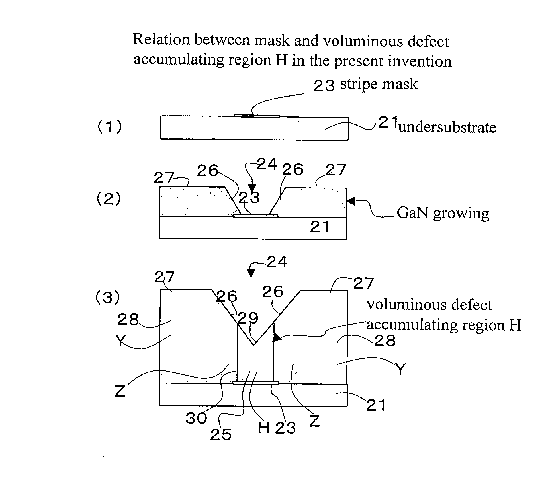
[0406] Undersubstrate O; a 30 mm q GaN undersubstrate which has been produced by Embodiment 1 based on Pattern A. This is a GaN mirror wafer without mask, which has been prepared by mechanically processing and mirror-polishing the GaN substrate made by Embodiment 1 as shown in FIG. 12(1). Although the GaN wafer of Undersubstrate O has no stripe mask, inherent components (H, Z and Y) play the role of the stripe mask.

[0407] Undersubstrate P; a 30 mmφ GaN / sapphire undersubstrate which has been prepared by growing a 2 μm thick GaN film on a sapphire undersubstrate by the MOCVD, depositing a 0.1 μm SiO2 film on the GaN film, and forming a stripe mask of Pattern A by photolithography.

[0408] The HVPE apparatus holds two undersubstrates O and P side by side on a susceptor and grows thick GaN films on the two undersubstrates O and P simultaneously on the same conditi...


PUM

PropertyMeasurementUnit
thicknessaaaaaaaaaa
thicknessaaaaaaaaaa
widthsaaaaaaaaaa

Abstract

A low dislocation density GaN single crystal substrate is made by forming a seed mask having parallel stripes regularly and periodically aligning on an undersubstrate, growing a GaN crystal on a facet-growth condition, forming repetitions of parallel facet hills and facet valleys rooted upon the mask stripes, maintaining the facet hills and facet valleys, producing voluminous defect accumulating regions (H) accompanying the valleys, yielding low dislocation single crystal regions (Z) following the facets, making C-plane growth regions (Y) following flat tops between the facets, gathering dislocations on the facets into the valleys by the action of the growing facets, reducing dislocations in the low dislocation single crystal regions (Z) and the C-plane growth regions (Y), and accumulating the dislocations in cores (S) or interfaces (K) of the voluminous defect accumulating regions (H).

Description

BACKGROUND OF THE INVENTION [0001] 1. Field of the Invention [0002] This invention relates to a single crystal gallium nitride (GaN) substrate, a method of growing single crystal GaN and a method of making a single crystal GaN substrate utilized as a substrate of making laser diodes (LDs) and light emitting diodes (LEDs) composed of groups 3-5 nitride semiconductors. [0003] This application claims the priority of Japanese Patent Applications No.2001-311018 filed on Oct. 9, 2001 and No.2002-269387 filed on Sep. 17, 2002, which are incorporated herein by reference. [0004] 2. Description of Related Art [0005] Light emitting devices based upon group 3-5 nitride semiconductor include blue / green light emitting diodes and blue light laser diodes. Blue light LEDs have been sold on the market. But, LDs have not been on the market yet. Almost all of the conventional 3-5 nitride light emitting devices and laser diodes (LEDs, LDs) have been fabricated upon sapphire (α-Al2O3) substrates. Sapphir...

Claims


Application Information

Patent Timeline
Patent Type & Authority Applications(United States)
IPC IPC(8): C30B23/00C30B25/00C30B28/12C30B28/14C30B23/02C30B29/38C30B25/02H01L21/20H01L21/205H01L33/32
CPCC30B23/02C30B25/02C30B29/403C30B29/406C30B23/002H01L21/20
Inventor MOTOKI, KENSAKUHIROTA, RYUOKAHISA, TAKUJINAKAHATA, SEIJI
Owner SUMITOMO ELECTRIC IND LTD
Why Eureka
Try Eureka