
Semiconductor device and manufacturing method of the same

Inactive Publication Date: 2007-04-19
SEMICON ENERGY LAB CO LTD
View PDF19 Cites 17 Cited by
  • Summary
  • Abstract
  • Description
  • Claims
  • Application Information

AI Technical Summary

Benefits of technology

[0021] A fundamental wave with a wavelength of about 1 μm is not absorbed so much by a semiconductor wafer in irradiating the semiconductor wafer with the fundamental wave. Thus, the fundamental wave has a low absorption efficiency. The present inventors have found that a fundamental wave emitted from a pulsed laser having a pulse width on the order of picoseconds, or on the order of femtoseconds (10−15 seconds) can provide high intensity laser light. Thus, a non linear optical effect (multiphoton absorption) is generated and the fundamental wave can be absorbed by the semiconductor wafer.
[0024] According to the present invention, a laser oscillator having a higher output power than 15 W, e.g., 40 W output power can be used for laser annealing, since a non-linear optical device is not used and thus light is not converted to a harmonic. Therefore, the width of an impurity region activated by one time laser-scanning can be increased, and thus the productivity can be enhanced dramatically.
[0028] In each of the above structures, the impurity regions are source and drain regions of a field effect transistor. An impurity element imparting an n-type conductivity to a semiconductor (such as As or P) or an impurity element imparting a p-type conductivity to a semiconductor (such as B) is added into the source and drain regions to reduce resistance. By selective laser irradiation, a desired region is only activated to reduce resistance.
[0040] By the present invention, a non-linear optical device for converting a wavelength is not needed, and a laser beam with an extremely high output power, for example, a laser beam having an energy of twice or more times as high as a harmonic can be obtained. Further, by the present invention, it is possible to prevent activated impurities from unnecessarily diffusing into a deep portion in a substrate. Therefore, impurities in an irradiated region can be activated efficiently in a state in which a semiconductor substrate is kept at a sufficient low temperature in recrystallization, and the element thus obtained is suitable for developing a higher performance device.
[0041] According to the present invention, an ultra shallow junction having a shallow junction depth can be formed. By forming an ultra shallow junction, leak current can be reduced, and low power consumption can be achieved. Further, miniaturization and high integration of a semiconductor integrated circuit become possible.
[0042] Further, a non-linear optical device has a defect that a maintenance-free state, which is an advantage of a solid state laser, cannot be kept long, since the non-linear optical device is easily changed in its quality. However, the present invention can overcome the defect, since the present invention does not need a non-linear optical device. In other words, stability and reliability of a laser irradiation apparatus itself can be enhanced, according to the present invention.

Problems solved by technology

A conventional laser annealing method using laser light oscillated from a pulsed excimer laser has some problems to be solved.
For example, there is a problem that crystal defects are generated in melting and recrystallizing by laser annealing.
However, in the case of using a CW laser and a quasi-CW laser using a solid state laser medium, the wavelength band of a fundamental wave is from red ray to near-infrared ray, and laser light absorption efficiency in the semiconductor is extremely low.

Method used


Image

  • Semiconductor device and manufacturing method of the same
  • Semiconductor device and manufacturing method of the same
  • Semiconductor device and manufacturing method of the same

Examples


embodiment mode 1

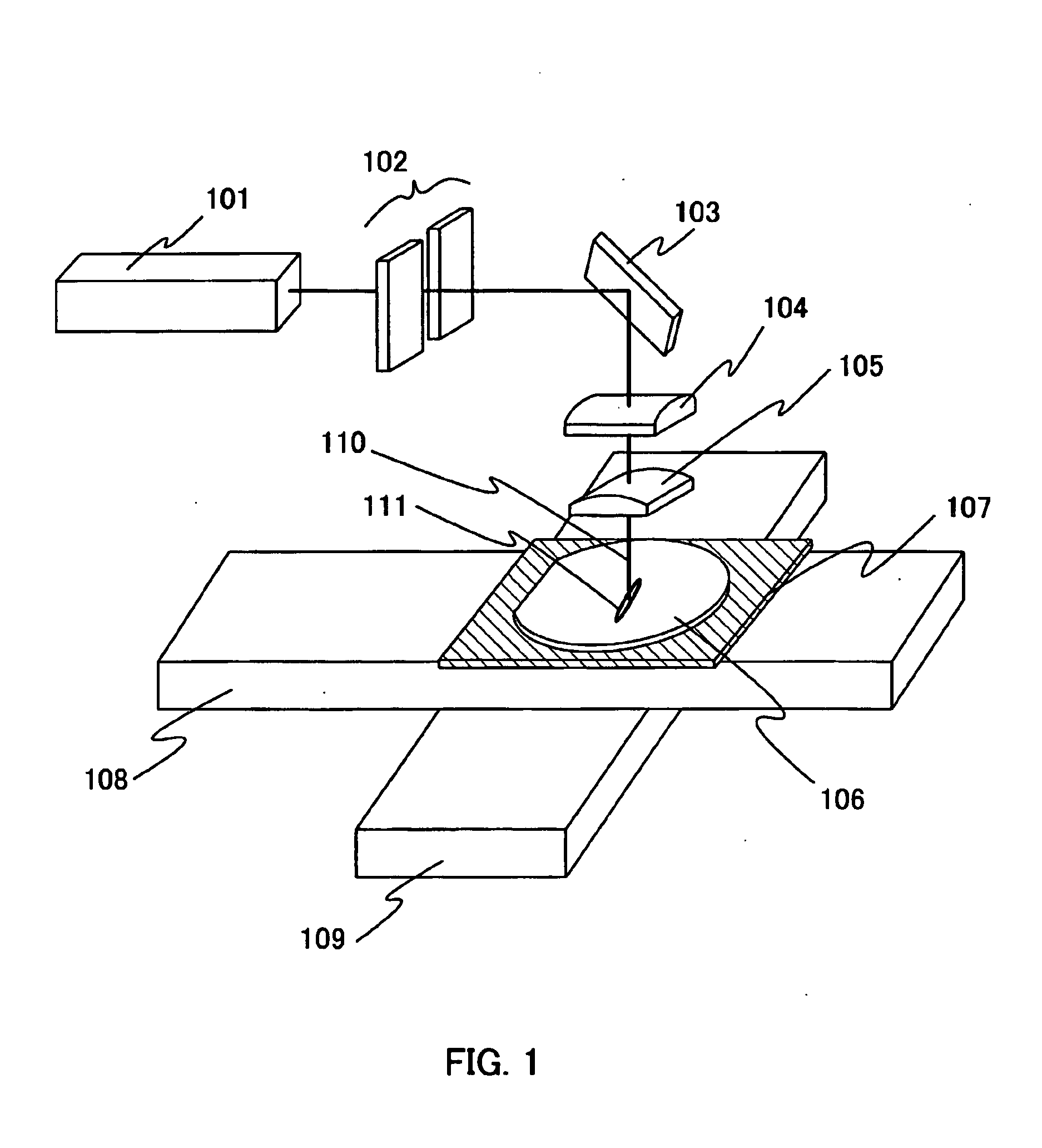
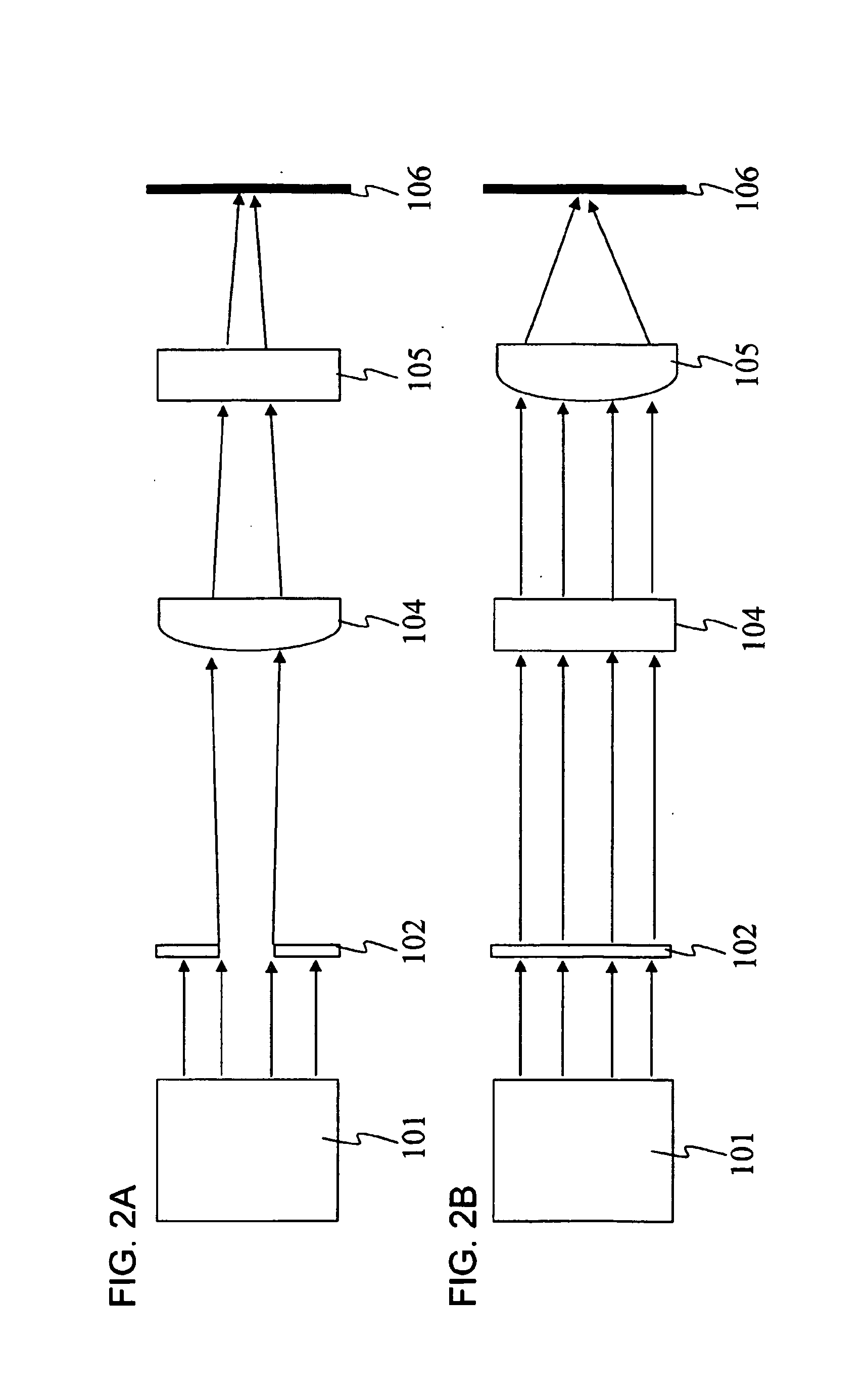
[0055]FIG. 1 is a perspective view showing one example of a laser irradiation apparatus according to the present invention.

[0056] As a laser oscillator 101 shown in FIG. 1, a laser oscillator which oscillates with a pulse width on the order of femtoseconds (10−15second) is used (also referred to as a femtosecond laser). As the laser oscillator, lasers in which Nd, Yb, Cr, Ti, Ho, Er, or the like is added as a dopant into a crystal of Sapphire, YAG, ceramics YAG, ceramics Y2O3, KGW, KYW, Mg2SiO4, YLF, YVO4, GdVO4 or the like can be given. Note that a non-linear optical device is not included in the laser oscillator 101 and thus the fundamental wave of a laser beam is emitted. A non-linear optical device for converting light oscillated from a laser medium to a harmonic is not included in the laser oscillator 101; however, the laser oscillator 101 has high enough light intensity to generate a non linear optical effect (multiphoton absorption) in a semiconductor.

[0057] First, a laser ...

embodiment mode 2

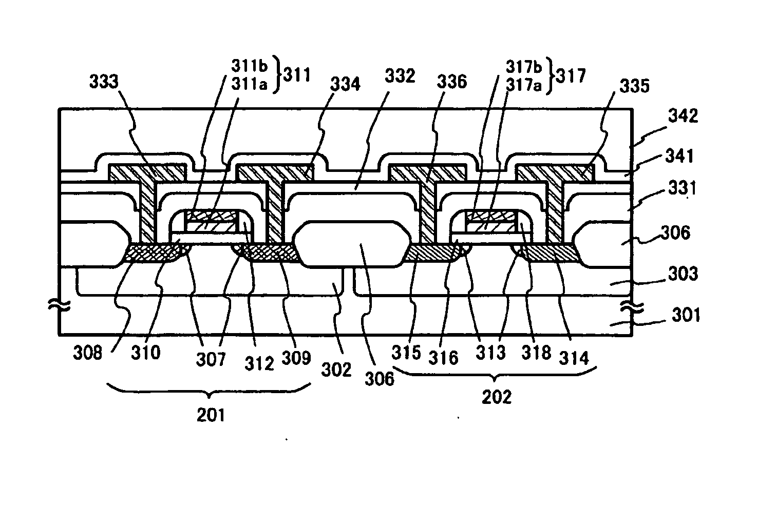
[0074] A procedure for manufacturing an FET using the present invention will be hereinafter described briefly with reference to FIGS. 3A and 3B. Here, an example of activation is shown, in which a non linear optical effect (multiphoton absorption) is produced in an irradiation region by irradiating an impurity region doped with impurities by laser light having a fundamental wave with a wavelength of a near-infrared region, and a pulse width of about 10 ps or less.

[0075] A silicon substrate 301 formed of single-crystal silicon is prepared. An n-well 302 is selectively formed in a first element formation region over a main surface (an element formation region or a circuit formation region) of the silicon substrate, and a p-well 303 is selectively formed in a second element formation region over the same surface.

[0076] Next, a field oxide film 306 to be an element isolation region for partitioning the first element formation region and the second element formation region is formed. T...

embodiment mode 3

[0092] A manufacturing method of a semiconductor device of the present invention is described with reference to FIGS. 4A to 7. Embodiment Mode 3 describes an example of employing an SOI (silicon on insulator) substrate in which an insulating layer and a single-crystal semiconductor layer are stacked.

[0093] As SOI substrates, for example, a SIMOX (separation by implanted oxygen) substrate can be given. A SIMOX substrate 510 is a substrate which is manufactured by embedding oxygen molecules into a portion slightly deeper than the surface of the single-crystal semiconductor layer, and oxidizing it at a high temperature, thereby forming an insulating layer and a single-crystal semiconductor layer on the insulating layer. The substrate is a stack of a first single-crystal semiconductor layer 511, an insulating layer 512, and a second single-crystal semiconductor layer 513 (FIG. 4A).

[0094] A manufacturing method of a semiconductor device of the present invention using a SIMOX substrate ...


PUM


Abstract

An RTA method has a limitation on miniaturization. The RTA method needs a heating time of several seconds, and has a risk that impurities are diffused into a deep portion, since a semiconductor substrate is heated at a high temperature. Thus, the RTA method has a difficulty in responding miniaturization which is expected in the future. According to the present invention, a fundamental wave is used without putting laser light into a non-linear optical device, and laser annealing is conducted by irradiating an impurity diffusion layer with pulsed laser light having high intensity and a high repetition rate, so as to electrically activate the impurities. By the present invention, a thin layer on the surface of a silicon substrate can be partially melted to conduct activation. Further, the width of the region activated by laser-scanning once can be increased, and thus the productivity can be enhanced dramatically.

Description

TECHNICAL FIELD [0001] The present invention relates to a manufacturing method of a semiconductor device, using a laser irradiation apparatus for irradiating an object with laser light. Specifically, the present invention relates to a semiconductor device having a circuit including a field effect transistor (hereinafter, referred to as an FET). Further, the present invention relates to electronic devices incorporating, as a part thereof, e.g., large scale integrated circuits (LSI), electro-optic devices typified by liquid crystal display panels, light-emitting display devices having an organic light-emitting element, sensor devices such as line sensors, or memory devices such as SRAM or DRAM. [0002] Note that semiconductor devices in this specification mean generic devices which can operate with use of semi-conductive characteristics, and the category includes all types of devices such as electro-optic devices, semiconductor circuits and electronic devices. [0003] In recent years, m...

Claims


Application Information

Patent Timeline
IPC IPC(8): H01L21/00H01L31/111H01L21/8232H01L29/74H01L21/335H01L29/43
CPCH01L21/268H01L21/823814H01L21/84H01L27/10814H01L27/10817H01L27/10873H01L27/11H01L27/14618H01L29/6659H01L2224/48091H01L2924/15183H01L2924/15311H01L2224/45144H10B12/315H10B12/318H10B12/05H10B10/00H01L2924/00014H01L2924/00H01L21/265H01L21/8234H01L21/18H01L27/088
Inventor TANAKA, KOICHIROYAMAMOTO, YOSHIAKI
Owner SEMICON ENERGY LAB CO LTD
Learn More