
Non-spherical semiconductor nanocrystals and methods of making them

a technology of semiconductor nanocrystals and nanocrystals, which is applied in the direction of crystal growth process, crystal growth process, polycrystalline material growth, etc., can solve the problems of long preparation time and the method requires long hours, and achieves desirable optoelectronic properties, high quantum yield, and large quantities

Inactive Publication Date: 2007-08-16
THE RES FOUND OF STATE UNIV OF NEW YORK
View PDF9 Cites 25 Cited by
  • Summary
  • Abstract
  • Description
  • Claims
  • Application Information

AI Technical Summary

Benefits of technology

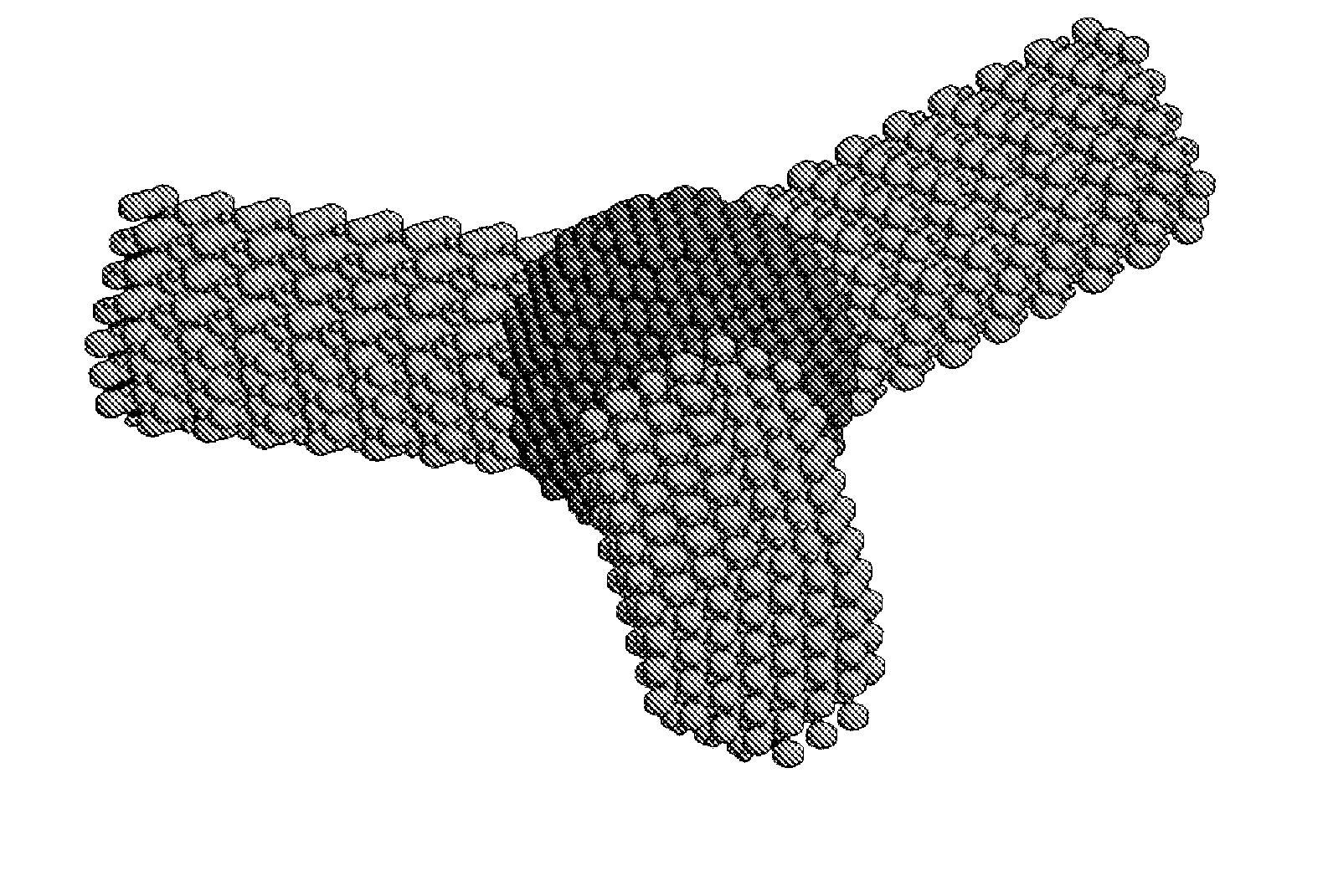
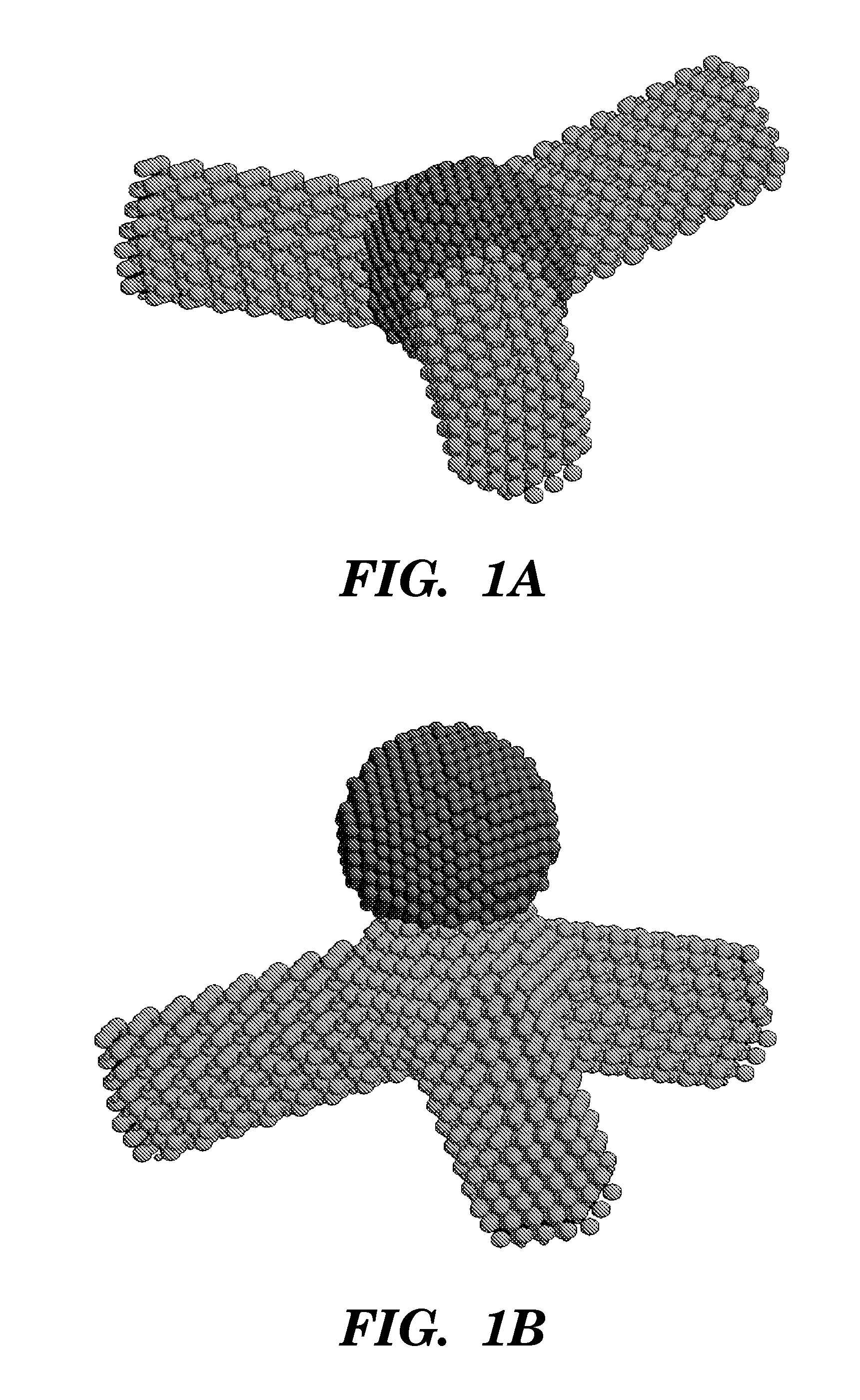
[0013] The method of the present invention has been optimized to produce high quantum-yield semiconductor nanocrystal rods and multipods in relatively large quantities and with desirable optoelectronic properties. The method of the present invention produces high chemical yields of the rod and multipod structures and high photoluminescence quantum yield. Reports in the scientific literature describe a general method for producing low quantum yield non-spherical semiconductor nanocrystals by using higher precursor concentrations and subsequently injecting the precursors into the reaction pot. Those methods require long hours of preparation. In contrast, the method of the present invention primarily addresses a facile one-pot synthesis approach to produce semiconductor nanocrystals of various aspect ratios with tunable optical properties by using noble metal nanoparticles as seeding agents. The aspect ratio of the nanocrystals can be easily tuned from ˜2 to ˜12. The high yield production and stability of high quantum yield of non-spherical semiconductor nanocrystals of the present invention will allow them to be used in applications in hybrid polymer solar cells, biological labeling, and other optoelectronics applications where high concentrations of highly stable nanocrystals are needed.
[0014] The method of the present invention also has the advantages of producing higher quality nanocrystals, indicated by the higher photoluminescence quantum yield which generally occurs due to good crystallinity and minimal surface trap states or crystal defects. Compared to the prevalent literature methods, these nanocrystals are made from less expensive and less toxic precursors, and from a simpler procedure. In accordance with the present invention, nonspherical nanocrystals can be obtained through a one-pot synthesis method without the use of phosphonic acids or trioctylphosphine oxide, the surfactants most often used for anisotropic growth of nanocrystals. The method of the present invention also does not require multiple precursor injections. The reaction temperature and reagent concentrations used in the method of the present invention are much lower than the ranges previously reported for non-spherical semiconductor nanocrystal synthesis, which are as high as 0.5-0.8 mmol per ml reaction mixture. The noble metal seed particles employed in the present inventive method facilitate nucleation and growth of nanocrystals at relatively mild conditions. The process is fast and can be finished within about 3 hours.

Problems solved by technology

Those methods require long hours of preparation.

Method used


Image

  • Non-spherical semiconductor nanocrystals and methods of making them
  • Non-spherical semiconductor nanocrystals and methods of making them
  • Non-spherical semiconductor nanocrystals and methods of making them

Examples


example 1

Materials

[0057] Cadmium oxide, myristic acid, 1-hexadecylamine, phenyl ether (99%), selenium, trioctylphosphine, tetraoctylammonium bromide (98%) (“TOAB”), hydrogen tetrachloroaurate(III) trihydrate (HAuCl4.3H2O), palladium chloride (PdCl2), sodium borohydride, dodecylamine, and phenyl ether were purchased from Sigma-Aldrich (St. Louis, Mo.). Silver nitrate (AgNO3) was purchased from Alfa Aesar (Ward Hill, Mass.). All chemicals were used as received. All solvents (hexane, toluene, and acetone) were used without any further purification.

example 2

Synthesis of Au, Ag, Pd, and Pt Nanoparticles

Au Nanoparticles

[0058] 20 mL of a bright yellow 5 mM HAuCl4 solution was mixed with 10 mL of a 25 mM TOAB solution. The mixture was vigorously stirred for 15 minutes. An immediate two-layer separation occurred, with an orange / red organic phase on top and a clear to slightly orange tinted aqueous phase on the bottom. The organic phase was separated into a glass vial and to it was added 5 mL of a 0. 12 g of dodecylamine in toluene solution, followed by dropwise addition of 5 mL of a 0.1 M of sodium borohydride solution to the stirring reaction mixture. An instant color change of the organic phase was observed from an orange-red to a deep-red color. The stirring was continued for 30 minutes. Following this, the organic phase containing gold nanoparticles was separated from the aqueous phase, and the organic phase was adjusted to 20 mL by adding additional toluene. In general, these particles were extremely soluble in toluene, chloroform, ...

example 3

Synthesis of CdSe Quantum Rods and Multipods

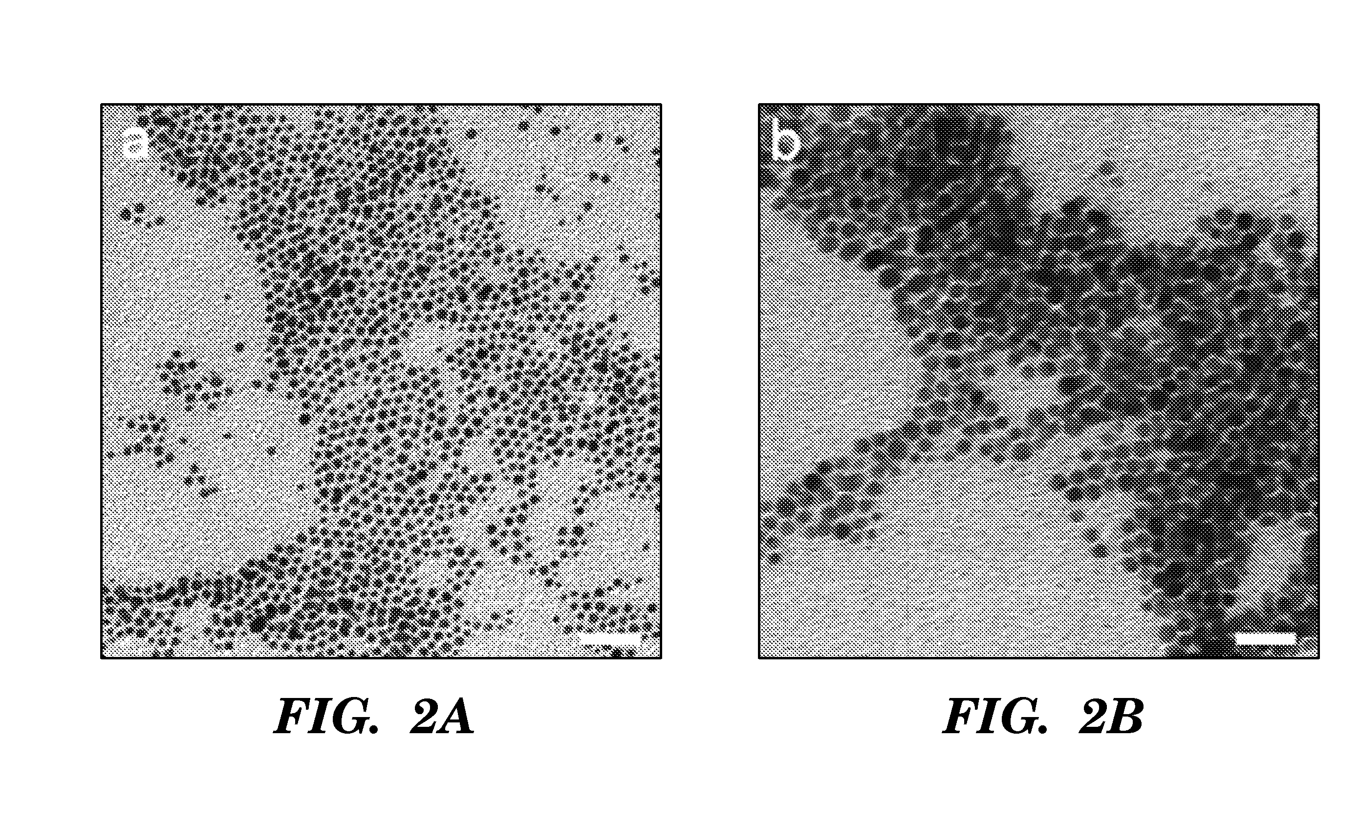
[0062] The following protocol was found to be optimal for obtaining CdSe quantum rods and multipods. 1 mmol cadmium oxide, 3 mmol myristic acid, 1 mmol hexadecylamine, and 15 ml phenyl ether were added into a 250 ml three-necked flask. 10 ml of freshly prepared metal nanoparticles (˜0.05 mmol metal atoms) in toluene was added. The reaction mixture was slowly heated under an argon atmosphere to 220° C., with a needle outlet that allowed the toluene to evaporate. After 20 minutes of heating, the needle was removed. The reaction mixture was maintained at 220° C. for another 20 minutes, then 0.5 ml of 1 M TOP-Se (0.5 mmol Se in 1.1 mmol trioctylphosphine) was rapidly injected. Approximately 1 ml aliquots were withdrawn after various reaction times. The aliquots were quenched with about 10 mL hexane. CdSe multipods and quantum rods were obtained at 1-3 minutes and 15-20 minutes, respectively.


PUM


Abstract

The present invention relates to a method of making non-spherical semiconductor nanocrystals. This method involves providing a reaction mixture containing a first precursor compound, a solvent, and a surfactant, where the first precursor compound has a Group II or a Group IV element and contacting the reaction mixture with a pure noble metal nanoparticle seed. The reaction mixture is heated. A second precursor compound having a Group VI element is added to the heated reaction mixture under conditions effective to produce non-spherical semiconductor nanocrystals. Non-spherical semiconductor nanocrystals and nanocrystal populations made by the above method are also disclosed.

Description

[0001] This application claims the priority benefit of U.S. Provisional Patent Application Ser. No. 60 / 752,445, filed Dec. 21, 2005, which is hereby incorporated by reference in its entirety.[0002] This work was supported in part by grant number F49620-01-1-0358 from the USAF / AFOSR. The U.S. Government may have certain rights.FIELD OF THE INVENTION [0003] The present invention relates to methods of making non-spherical semiconductor nanocrystals and non-spherical semiconductor nanocrystals made by the methods. BACKGROUND OF THE INVENTION [0004] Semiconductor nanocrystals have emerged as an important class of materials because of their tunable optoelectronic properties that arise from quantum size effects. They can be used as active components in functional nanocomposites (Morris et al., “Silica Sol as a Nanoglue: Flexible Synthesis of Composite Aerogels,”Science 284:622-624 (1999)), chemical sensors (Kong et al., “Nanotube Molecular Wires as Chemical Sensors,”Science 287:622-625 (20...

Claims


Application Information

Patent Timeline
IPC IPC(8): C30B13/00C30B19/00
CPCB82Y30/00C30B7/00C30B29/60C30B29/48C30B29/46C30B13/00C30B19/00
Inventor YONG, KEN-TYESAHOO, YUDHISTHIRASWIHART, MARKPRASAD, PARAS
Owner THE RES FOUND OF STATE UNIV OF NEW YORK
Learn More