

Integrated Semiconductor Bioarray
a bioarray and semiconductor technology, applied in biochemistry apparatus and processes, instruments, library screening, etc., can solve the problems of affecting the target-specific signal affecting the settling time of the system, and affecting the accuracy of the captured target,
- Summary
- Abstract
- Description
- Claims
- Application Information
AI Technical Summary
Benefits of technology
Problems solved by technology
Method used
Image

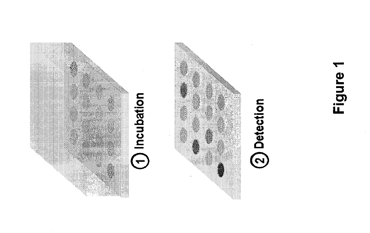
Examples
example 1
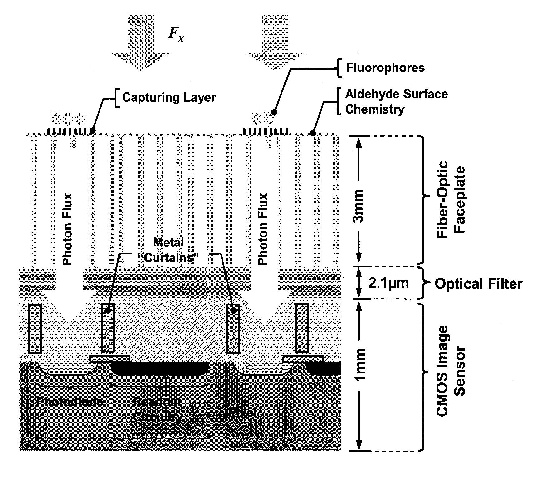
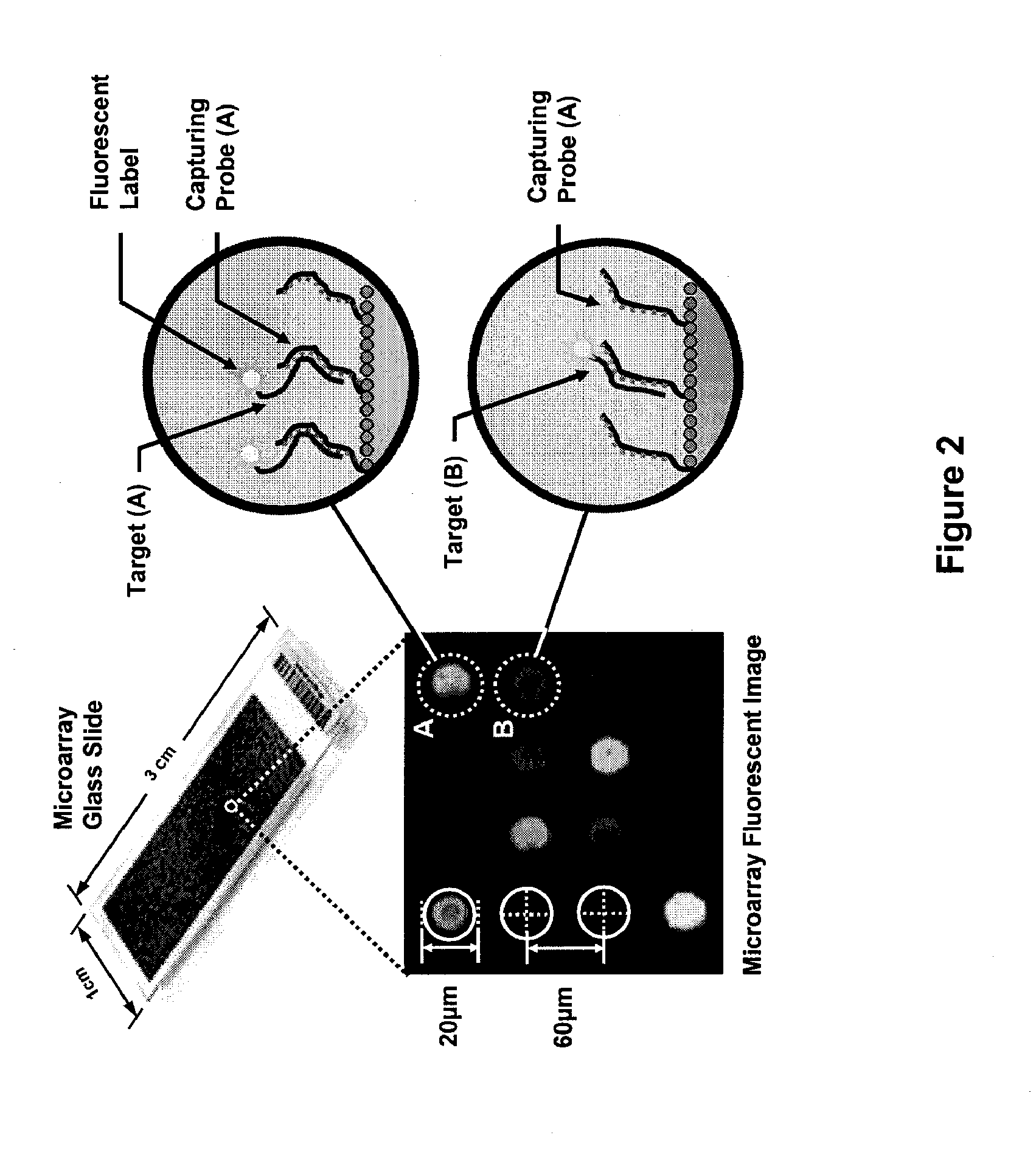
[0218] This example illustrates how an optical filter layer in the form of a band-pass filter on the surface of the CMOS chip enhances optical performance of the integrated biosensor array. A challenge of designing any fluorescent-based detector is the proper optical excitation and detection of fluorescent labels. FIG. 9 illustrates the absorption and emission spectra of Cy3 molecule which is an example fluorophore of a system. The absorbed photon density for Cy3, denoted by A, exposed to the incident photon flux, FX, obeys the Beer-Lambert law. For a thin layer of diluted absorbing media with Cy3 as in microarray applications we have
A=FX[1−e−a0(λ)N]≈FXa0(λ)N, (1)
where a0(λ) and N are the extinction coefficient in wavelength λ and surface concentration of Cy3 respectively. Considering QY, the fluorescence quantum yield of Cy3, we can calculate IE, the total emitted photons per surface area by
IE=QYA≈QYFXa0(λ)N (2)
[0219] As evident in FIG. 9, the photon emission is, to first or...
example 2
[0220] This example describes the construction of a fully integrated biosensor array of the present invention. To design the CMOS photo-detector a Nwell / Psub photodiode array is used in the 0.35 μm CMOS process. Each diode is 50 μm×50 μm and the array pitch is 250 μm. This dimension is compatible with commercial microarray specifications and also minimizes the optical cross-talk between photodiodes while providing sufficient space to integrate in-pixel a photocurrent detector and an analog to digital converter (ADC).
[0221] Most of the CMOS image sensors use direction integration, where the photocurrent is directly integrated over a reverse bias photodiode capacitor. In the design, a capacitive transimpedance amplifier (CTIA) in the pixel is used as a photocurrent integrator. Comparing with a CTIA, a direct integrator suffers from the junction capacitance variation as the reverse bias voltage changes depending on the output signal level. A CTIA does not have any such problems since ...
PUM
| Property | Measurement | Unit |
|---|---|---|
| Thickness | aaaaa | aaaaa |
| Thickness | aaaaa | aaaaa |
| Thickness | aaaaa | aaaaa |
Abstract
Description
Claims
Application Information