

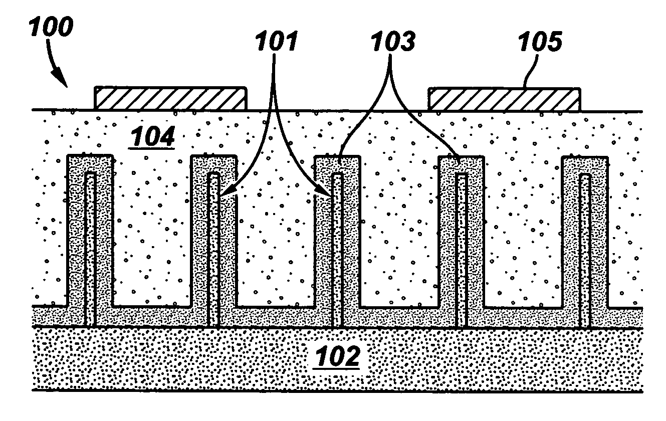
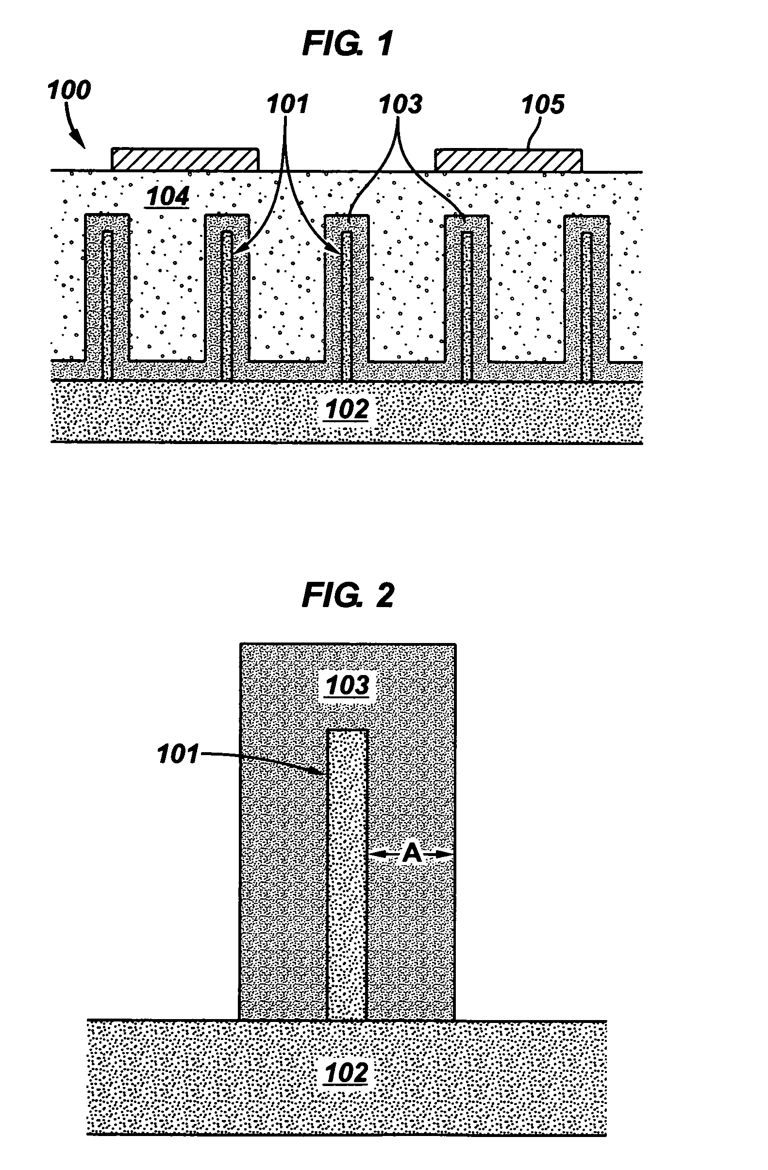
Graded hybrid amorphous silicon nanowire solar cells
a hybrid amorphous silicon nanowire and solar cell technology, applied in the field of photovoltaic devices, can solve the problems of limiting the conversion efficiency of a standard cell to about 44%, no efficient enough to significantly reduce the cost involved in the production and use of this technology, and the competition from conventional sources of electricity precludes the widespread use of such solar cell technology, etc., to achieve enhanced voc and isc, high conversion efficiency, and increase collection efficiency
- Summary
- Abstract
- Description
- Claims
- Application Information
AI Technical Summary
Benefits of technology
Problems solved by technology
Method used
Image

Examples
example 1
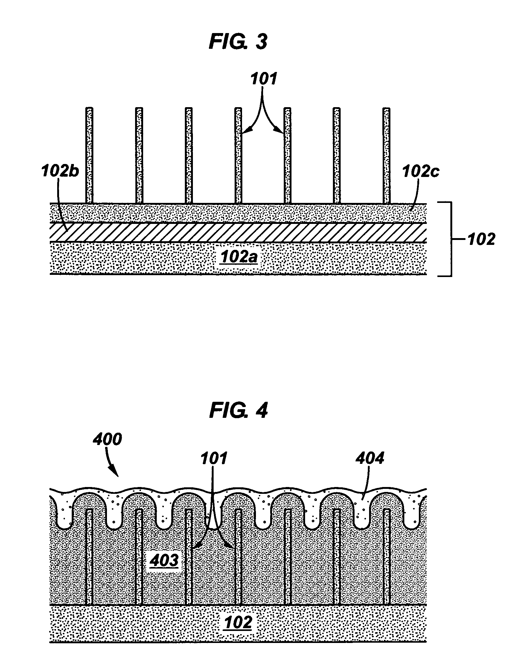
[0071]This Example serves to illustrate process steps for fabricating compositionally graded hybrid nanowire photovoltaic devices, in accordance with some embodiments of the present invention.
[0072]Silicon nanowire films of one conductivity type on glass, metal, or semiconductor substrate are placed in a plasma reaction chamber (e.g., a plasma enhanced chemical vapor deposition system). A vacuum pump removes atmospheric gases from the chamber. The substrates to be processed are preheated to 120-240° C. A hydrogen plasma surface preparation step is performed prior to the deposition of the compositionally graded layer. H2 is introduced into the chamber at a flow rate of 50-500 sccm (standard cubic centimeters per minute). A throttle valve is used to maintain a constant processing pressure in the 200-800 mTorr range. Alternating frequency input power with a power density in the 6-50 mW / cm2 range is used to ignite and maintain the plasma. Applied input power can be from 100 kHz to 2.45 ...
example 2
[0076]This Example serves to illustrate an exemplary application in which photovoltaic device 100 (or variants thereof) may find use, in accordance with some embodiments of the present invention.
[0077]Photovoltaic modules containing a plurality of photovoltaic devices 100 are typically mounted onto the roofs of homes for grid-connected power generation. The modules are mounted by several methods to yield functional and aesthetic qualities. The module provides power that may be stored or sold back to the electric company for a profit, as is currently done with standard residential solar cell modules. The solar cells may be cut into standard sizes and mounted in a module frame and connected in series using standard solder-based interconnect schemes, in some cases with bypass diodes to minimize shading effects. In cases where the nanowires are grown on a transparent material, the full glass substrate may be directly used in the framed module, or the glass may be laminated and used as t...
PUM
 Abstract
Description
Claims
Application Information